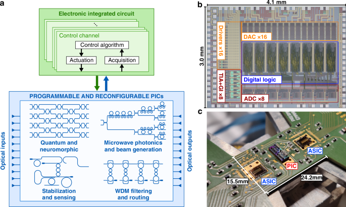
The 8-channel CMOS electronic integrated circuit has been specifically designed for dynamically controlling programmable optical circuits implemented in Silicon Photonics technology. The ASIC has been conceived to operate PICs whose functionality is defined by completely switching on/off optical interconnections, implemented with Mach-Zehnder interferometers. When dealing with MZIs, each channel of the controller simultaneously drives two thermo-optical actuators; however, the chip can also be effectively employed to control microring resonator (MRR) based circuits, where only one actuator is needed, as well as combinations of MZI and MRR and any other photonic circuit. Figure 1b shows a microscope photograph of the CMOS controller. The ASIC, built in AMS CMOS 0.35 μm technology, occupies an active silicon area of ≈12 mm2, thus comparable to the photonic chip. The power dissipation of each electronic channel, working with 3.3 V power supply, is ≈ 10 mW, less than what a single thermal actuator requires to achieve a phase shift larger than 2π, in the order of ≈30 mW (measurements are provided in Supplementary Section 4). Given the compact size of the electronic chip, multiple ASICs can be connected to a single PIC whenever more than 8 channels have to be managed in parallel. Figure 1c shows the connection between two ASICs and a PIC (described in detail in the following section), made through direct wire bonding to minimize the effect of stray capacitance, maximize the readout accuracy and limit the assembly size. A custom printed circuit board (PCB) has been designed to host the chips during the experimental validation, route the electrical signals necessary for their operation and communicate with a personal computer to configure and monitor the system.
The architecture of the electronic control channel is shown in Fig. 2a. The optical power impinging on one output branch of the photonic device is read by an integrated photodiode (PD). In this work, we consider germanium PDs that are commonly provided by foundry process design kits, but other kinds of PDs or monitor photodetector19 can be used as well by properly adapting the circuit. The photogenerated current is fed to the analog front-end of the ASIC for amplification through a transimpedance amplifier, low-pass filtering with a gated integrator and digitization by a 10-bit analog-to-digital converter (ADC) working with sampling rate fs = 100 kSamples/s. An input optical power dynamic range of 50 dB has been considered during the design of the analog acquisition chain to correctly detect the photogenerated current (≈30 dB to account for the MZI/MRR rejection ratio, plus an additional margin of 20 dB to adapt to possible coupling losses and different optical power levels). The gain of the front-end stage is automatically selected by a digital logic among 6 different values according to the absolute optical power impinging on the photodetector, in order to always match the ADC full-scale range to the photocurrent level. Optical signals between 0 dBm and −50 dBm can thus be successfully detected and managed by the ASIC, suitable for realistic applications. This is confirmed by the experimental measurement shown in Fig. 2b, which reports the values sampled by the ADC as a function of the input PD current and highlights the operation of the adaptive amplification stage.
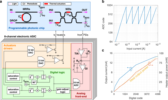
a Schematic view of the ASIC architecture for dynamic control of programmable photonic circuits. The ASIC features 8 parallel channels. b Measured ADC code for a wide range of input currents, that can be correctly detected thanks to the adaptive amplification mechanism. c Characterization of the actuator driver circuit: the square root compression of the DAC output (blue) results in a linearization of the heater dissipated power (red) with respect to the digital control value
The control algorithm to maximize/minimize the optical power at the output of each photonic device, needed to switch on/off the desired optical paths, is implemented at digital level and relies on the dithering technique in combination with integral controllers20. This approach allows to define a feedback strategy that is easily scalable to multiple devices and independent of the average light power in the chip and the setup temperature. The error signal minimized by the lock-in based control loop is only related to the partial derivatives of the optical output power with respect to the actuators command: it is thus insensitive to any DC offset, that might result from the sensors dark current or the residual optical power injected from other devices in the PIC (more details on the control algorithm are provided in Supplementary Section 1). The dithering extraction and integration processes are performed in the digital domain, to increase chip flexibility. Two independent chains operating on orthogonal dithering signals are needed when controlling MZIs with two heaters, whereas a single digital circuit is enough for a MRR. Within each chain, a square-wave multiplier downconverts the ADC readout and a digital integrator accumulates the resulting signal, thus simultaneously implementing the integral feedback law needed for controlling the photonic device and precisely defining the control loop bandwidth. The obtained DC signal, upon which the square-wave oscillation is superimposed to apply the dithering modulation to the actuators, is used to update the device working point. A square root operator, whose details are described in Supplementary Section 4, is used to compress the generated digital word and linearize the feedback loop, by compensating the quadratic relation between the heater voltage and its dissipated power. This ensures the same control loop response regardless of the actuators DC bias14. The output digital word is finally compared with two programmable thresholds, that trigger the reset of the accumulator at mid-scale in order not to saturate the driving circuit when the generated voltage gets too close to the power supply rails.
The output of the digital logic is fed to a mixed-signal actuation circuit, made of a pair of 12-bit digital-to-analog converters (DACs) and high-current analog drivers. The drivers are designed to operate the integrated thermal phase shifters, which have a nominal resistance RH ≈ 400 Ω, within a 0–6 V range, corresponding to a maximum phase shift of ≈4π. In this way, the control loop is always able to find a minimum in the device transfer function regardless of the algorithm starting condition. The resolution of the DACs has been chosen to achieve an accuracy of ≈ 1.5 mV in the generation of the actuators voltage, enough to perform an effective control action. Figure 2c shows the measured current provided by the driving stage to the actuators, and the corresponding heater dissipated power, confirming the effective linearization performed by the square root operator and the sufficient power capability of the circuit.
Integrated 16-channel self-aligning beam coupler
The designed ASICs have been used to dynamically control a 16-channel silicon photonics integrated self-aligning universal beam coupler (UBC). UBCs are a class of reconfigurable PICs that can receive an arbitrary monochromatic input beam and couple it to a single-mode waveguide17,18. They can be implemented as a combination of 2 × 2 interferometers, such as Mach-Zehnder interferometers (MZIs), arranged in a mesh configuration10,21. By making each interferometer tunable with proper on-chip actuators, an adaptive UBC can be dynamically reconfigured to work as a coherent intensity adder and constantly maximize the input-output coupling efficiency even when the input beam characteristics change. The reconfigurability of UBCs makes them suitable to track and mitigate the effect of dynamic phenomena, such as time-varying angular misalignments (i.e., direction of arrival) between an input beam and the photonic chip and/or wave-front distortions caused by propagation through aberrators, scattering media, multimode or multicore fibers/waveguides or turbulent environments, as in the case of atmospheric turbulence in free-space optical (FSO) links22.
A schematic of the designed integrated photonic circuit and its top-view microscope photograph are shown in Fig. 3a, b. The circuit has been manufactured by a commercial silicon photonic foundry (Advanced Micro Foundry, Singapore) and has an area of 3.2 mm × 1.3 mm. It consists of 15 thermally-tunable balanced MZIs arranged in a 4-stage 16 × 1 binary mesh. Compared to other mesh topologies17,21, this arrangement equalizes the optical path from all inputs to the output and minimizes the number of cascaded MZI stages, thus resulting in a faster configuration time for the receiver. At the input (left-hand side in Fig. 3a), the MZI mesh is connected to an integrated 16-element optical antenna array (OAA). The antennas are realized by using surface grating couplers (GCs) designed to operate on transverse-electric (TE) polarized light. The 16 GCs are arranged in two concentric rings with a radius of 60 μm (inner ring, 7 GCs) and 180 μm (outer ring, 8 GCs), respectively, and a central GC, as shown in Fig. 3b. This OAA configuration is optimized to receive optical beams with a linear polarization and circular symmetry, but other OAA topologies can be designed for other classes of beams23. Waveguide stubs are inserted between the OAA and the MZI mesh to match the length of each input optical path and minimize the wavelength dependence of the UBC21 (see Methods for further details). At the output of the MZI mesh, 15 waveguides are coupled to integrated photodetectors, while the 16th waveguide (optical output) is terminated with a GC for coupling with an optical fiber.
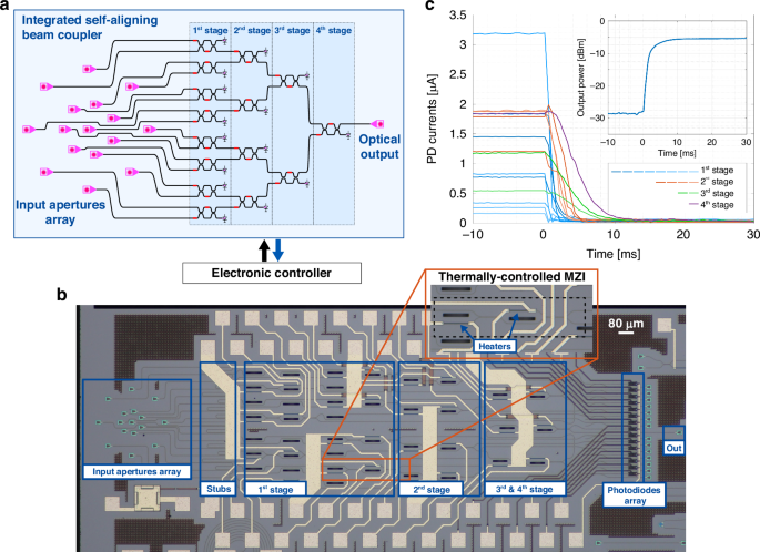
a Schematic view and b microscope photograph of the self-configuring optical beam coupler, made of a binary-tree mesh of 15 MZIs. A detail of a thermally-tunable MZI, featuring two actuators to completely steer the input light to one of the device outputs, is also reported. c Time transient of the PDs photocurrents when configuring the optical circuit, showing correct minimization when the ASICs are activated after 10 ms. The inset shows the evolution of the chip output power, which is correspondingly maximized in around 10 ms
Two ASICs have been used to control the UBC. To demonstrate the possibility of configuring the photonic circuit starting from any initial condition, heater voltages have been initially set to random values; then, the 16 control loops have been simultaneously activated. Figure 3c shows the measured PD currents during the configuration transient of the photonic circuit. All photocurrents are minimized by the ASICs, thus steering all the input light towards the chip optical output. The configuration of the first stage of the receiver takes place in around 1.5 ms, while the following layers are characterized by a slightly longer convergence time. In fact, the Nth stage of the mesh cannot be completely tuned before all the previous N−1 stages have been set. This is visible in the figure, which highlights the sequential tuning of the circuit. Even with 4 cascaded stages, the electronic ASICs can configure the whole MZI architecture in around 10 ms, as shown by the transient of the optical output power in the inset of the figure. It is worth pointing out that all MZIs are configured by using the same dithering frequency. This approach simplifies the control electronics and does not prevent correct configuration of the PIC. Indeed, once the MZIs of the Nth stage are locked to the minima/maxima of their transfer function, they do not inject any disturbance to the Nth + 1 stage, since the residual dithering oscillation at their output is nil in stationary points.
Dynamic correction of wavefront distortions
The performance of the ASIC controller was assessed by testing the UBC as a dynamic tracker of wavefront distortions of free-space optical beams. In the first experiment (Fig. 4a), static distortions with a well-controllable profile were intentionally introduced by means of a spatial light modulator (SLM) placed along the propagation path of the beam (see Methods and Supplementary Section 2 for details on the experimental setup). The SLM was used to generate 15 synthetic phase masks (reported in Supplementary Section 3) and an infrared camera was used to capture the resulting perturbation effects. As reported in Fig. 4b, the Gaussian profile of the input beam (left panel) is significantly altered after reflection on the SLM, with a significant change of shape, size, and centroid (right panel). The distorted beam was coupled to the OAA of the PIC through a collimating lens. The performance of the ASIC-controlled PIC was then assessed by measuring the optical power at the output port of the UBC when the ASIC control is switched off (all the heaters are held at a constant voltage) and when the feedback control is activated to find the best mesh configuration and maximize the output power. Figure 4c shows the optical output power for different phase screens of the SLM (data are normalized to the output power received when SLM is off and no perturbation is introduced). When the control is turned off, the average received power is −5.7 dB with a standard deviation of 2.9 dB. Instead, when the UBC is automatically reconfigured after changing the SLM mask, the average power improves to −0.8 dB and the standard deviation reduces to 0.6 dB, thus demonstrating the effectiveness of the adaptive ASIC controller. The slight residual fading is due to the shift of the centroid of the beam causing variations of the total power impinging on the GCs of the OAA under different perturbation profiles. This can be improved with a larger OAA and with a higher fill factor, obtained by employing more GCs, an array of lenslets or a photonic lantern device21.
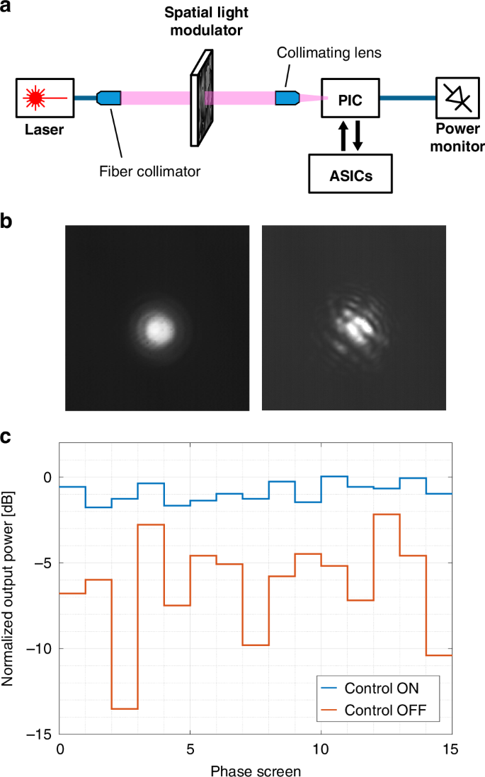
a Schematic view of the setup employed to introduce a static perturbation in the wavefront of a free-space beam. b Photograph, captured with an infrared camera, of the optical beam impinging on the beam coupler, when the SLM is off (left) and when it is used to perturb the free-space beam (right). c Optical power at the output port of the beam coupler for different SLM phase screens, showing its ability to perform real-time wavefront correction and beam reconstruction
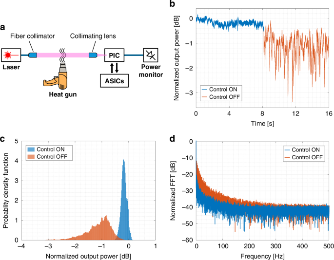
To test the ASIC controller in dynamic conditions with fast wavefront distortions of the optical beam, the SLM was replaced with a heat gun introducing turbulence in the free space path (Fig. 5a). Figure 5b shows the measured power at the optical output of the PIC when the control ASICs are activated (blue curve) / deactivated (orange curve) (data are normalized to the output power received when the PIC is configured for an unperturbed Gaussian beam, obtained with the heat gun turned off). When the ASICs are on, the UBC compensates for the wavefront distortion and the detected optical power at the output has a mean value of −0.17 dB, a standard deviation of 0.1 dB and a maximum fading of less than 0.5 dB. After 8 s, the control loops are paused, by holding the heater driving voltages at fixed values. In this condition, the PIC is on average well configured to receive the incoming beam, however the random phase front fluctuations result in a degradation of the received power: a mean value of −1.15 dB and a standard deviation of 0.5 dB are observed, with a maximum fading higher than 3 dB. The same is clearly visible in Fig. 5c, which compares the probability density function of the received optical power in the two situations. These results confirm the advantage of dynamic and real-time PIC reconfiguration, which translates in a narrower distribution concentrated at higher power levels: 90% of the samples are above the threshold of −0.3 dB when the controller is tracking the injected turbulence, whereas the same parameter worsens to −1.83 dB when no control is exerted (and only ≈ 1% of the samples stay above −0.3 dB). Figure 5d shows the frequency spectrum of the optical signal at the output waveguide of the UBC. When the control loops are off (orange curve), spectral components extending up to about 300 Hz are observed, which are related to the harmonics of the perturbation generated by the heat gun. The spectrum acquired after the activation of the ASIC controllers (blue curve) confirms that the real-time reconfiguration of the PIC significantly reduces the perturbation effect on the output up to around 300 Hz. This demonstrates that the tracking time of the ASIC-controlled PIC is faster than 10 ms. Notably, this response time is faster than the dynamics of atmospheric turbulence24, meaning that our approach can be effectively used to compensate for wavefront distortion in real free space links for communication, sensing and ranging applications.
a Experimental setup employed to introduce a dynamic perturbation in the free-space propagation of the beam. b Temporal evolution, c probability density function, and d frequency spectrum of the received optical power when the ASICs are active (blue curves) or disabled (orange curves), demonstrating correct real-time compensation of the beam-front distortion performed by the electronically controlled photonic chip
ASIC-assisted adaptive free-space optical receiver
The ASIC-assisted UBC was finally employed to receive a high-data-rate free-space optical signal corrupted by wavefront distortions. To this aim, the laser beam was modulated in intensity at a symbol rate of 25 Gbaud with a commercial modulator and transmitted through a free-space optical link. As in previous experiments, at the receiver side the optical beam was coupled to the OAA of the UBC, whose optical output was captured with a single-mode optical fiber and monitored with a real-time optical oscilloscope to assess the signal quality. No signal equalization has been performed. The results of the data transmission experiment are shown in Fig. 6a, for the case of 25 Gbit/s non-return-to-zero on-off keying modulation. When the working point of the photonic processor is not optimized by the ASICs (bottom panel), the input beams sampled by the OAA are combined along the MZI mesh with random phase relations, resulting in a degraded signal with a completely closed eye diagram at the chip output. In contrast, a fully open eye diagram with a quality factor of 6.12 is recorded when the ASIC controllers are activated. Notably, the control of the coherent adder performed by the ASIC controller is independent of the modulation format and data rate of the transmitted signal. Figure 6b shows the eye diagrams of a 50 Gbit/s 4-level pulse-amplitude modulation (PAM-4) with (upper panel) and without (lower panel) adaptive PIC configuration, confirming a clear improvement of the quality of the received signal when the ASIC controller is activated.
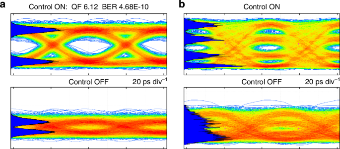
Eye diagrams of the received optical signal when transmitting a free-space beam modulated at 25 Gbaud both with a OOK and b PAM4 modulations, showing the transmission improvement when the adaptive receiver is dynamically operated