The design process started with three key steps. First, a single element was designed to operate in the X and Ku bands. Next, parasitic elements are added to the proposed design. Finally, the elements were arranged into a 1 × 4 array.
Sub-element designKu band Element
The conventional type of microstrip planar antenna is a rectangular patch due to its simplicity and reliable performance. The rectangular patch can be conceptually viewed as a two-aperture radiator with a λg/2 spacing between its effective radiating edges, supporting the fundamental TM10 mode. To enable miniaturization without altering the aperture separation, four identical square slots are etched at the patch perimeter. These slots act as reactive LC loads, compelling the surface current to follow a longer path, effectively increasing the electrical length. This slow-wave effect reduces the resonant frequency while maintaining the same outer dimensions, resulting in a compact dual-band antenna30. However, a patch antenna typically offers a narrow bandwidth, unsuitable for radar systems. Several techniques can enhance bandwidth, such as aperture feeding, which significantly increases bandwidth. Aperture feeding consists of two substrates: a ground plane, a radiating patch, and a microstrip feed line. In this design, as shown in Fig. 1a,b, and c, a folded rectangular patch is placed on a top substrate of Rogers 5880 with a permittivity of 2.2 and a height of 1.57 mm. The feed is located on a bottom substrate of Rogers 4350B with a permittivity of 3.48 and a height of 0.762 mm. These two substrates are separated by a ground plane with a rectangular slot (aperture feed), shielding the antenna on the top substrate.
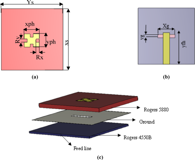
Single element works at Ku band. (a) Top substrate. (b) Back of 2nd substrate. (c) 3D design of single element.
To systematically arrive at the optimal geometry of the Ku-band antenna element, a progressive design methodology is adopted through a multi-step design process as shown in Fig. 2a. First, the design begins with a conventional rectangular microstrip patch antenna, which initially exhibits poor impedance matching. To improve performance, two slots are introduced at the center of the horizontal edges of the patch, resulting in enhanced matching characteristics and reducing antenna size. Subsequently, two more square slots are added to the vertical edges to further reduce the antenna profile. The complete sequence of these three design steps leads to the final shape. Figure 2b shows the simulated reflection coefficients of all steps.
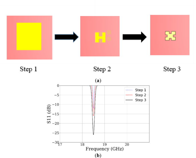
(a) Design steps of Ku-band element. (b) Simulated reflection coefficients of the design steps.
Impedance matching was achieved by tuning the feed-stub length, aperture slot dimensions, and ground-slot width. Varying the length of the four edge-centered square slots from 0.64 to 1.04 mm revealed that a length of 0.84 mm provides optimal matching, as shown in Fig. 3a. Additionally, a parametric sweep of the ground-plane slot width (Xg) from 1 to 5 mm identified 5 mm as the best value, as illustrated in Fig. 3b. These optimized parameters were adopted in the final antenna design.
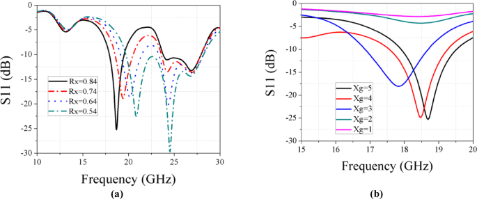
(a) Parametric analysis on Rx at Ku band. (b) Parametric analysis on Xg at Ku band.
This configuration achieves a bandwidth for the Ku band ranging from 17.9 to 19.5 GHz, as explained in Fig. 4a. Antenna achieves a gain of 8.12 dBi for the stated band. In Fig. 4b, the simulated radiation pattern at the Ku band is illustrated.
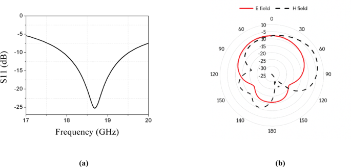
(a) Simulated results of S11 at Ku band. (b) Simulated E and H field patterns at Ku band.
X band Element
To adapt the design for the X-band, the Ku-band patch was scaled up by increasing its dimensions, as shown in Fig. 5a,b, and c. An additional rectangle was subtracted from each corner of the main patch to reduce its size. The optimized antenna dimensions are Cy = 2.5 mm as illustrated in Fig. 6.
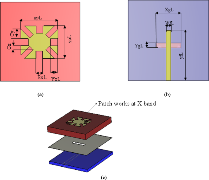
Single element works at X band. (a) Top substrate. (b) Back of 2nd substrate. (c) 3D design of single element.
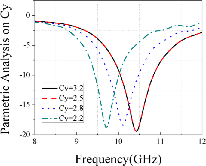
Parametric analysis on Cy at X band.
The ultimate shape of the X-band single-element antenna is obtained through a step-by-step design process similar to the Ku-band element, with an additional final stage for optimization, as shown in Fig. 7a. In the last step, corner sections are removed to enhance performance and further reduce size. The simulated reflection coefficients are presented in Fig. 7b. The resulting bandwidth in the X band is approximately 0.61 GHz, demonstrating good impedance matching at 10.5 GHz as illustrated in Fig. 8a. A gain of 4.862 dBi is achieved. Figure 8b presents the simulated radiation pattern.
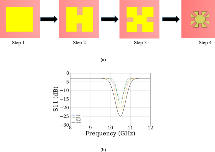
(a) Design steps of single X-band antenna element. (b) Simulated S₁₁ results at each step.
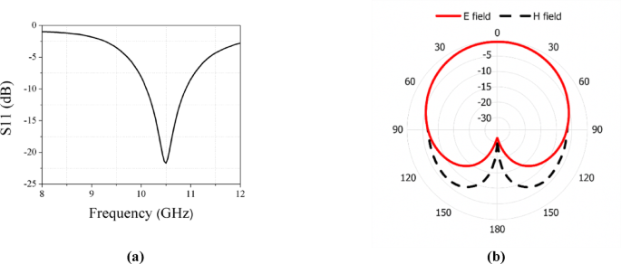
(a) Simulated results of S11 at X band. (b) Simulated E and H fields patterns at X band.
MIMO configuration
To support multi-band operation and polarization diversity, a MIMO configuration is first constructed. The design consists of two vertically polarized X-band elements forming a two-port MIMO system, along with a centrally positioned, one horizontally polarized Ku-band element, as illustrated in Fig. 9a,b. Next, an additional Rogers 5880 substrate (with a permittivity of 2.2 and a thickness of 1.57 mm) is incorporated at the top of the structure. This substrate serves as a base for the four parasitic patches per band, effectively suppressing adjacent mode excitation. For compactness, each pair of driven patches for each operating band shares two parasitic patches. The 3D representation of the final MIMO configuration is shown in Fig. 9c.
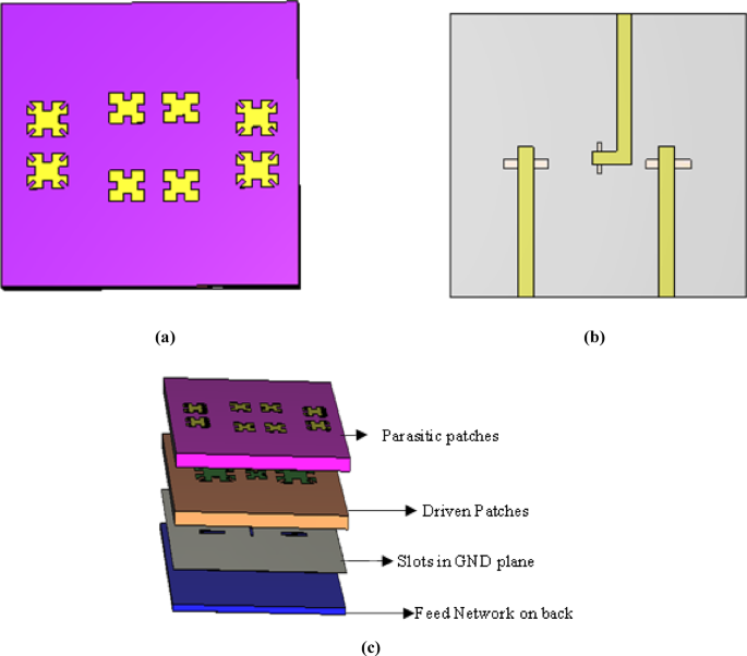
MIMO configuration. (a) Parasitic patches and driven patches. (b) Back of 3rd substrate. (c) 3D design of MIMO configuration.
For the X-band MIMO configuration, the design operates at 9 GHz, with a gain of 6 dBi and bandwidth of 0.5 GHz. For the Ku-band, the design achieves optimal performance at 16 GHz, with a gain of 10.1 dBi and a bandwidth of 1.5 GHz, as shown in Fig. 10a,b respectively. Figure 10c demonstrates the coupling between elements.
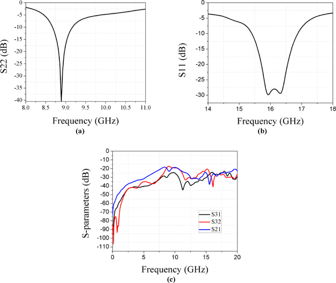
(a) Simulated results of X band in MIMO. (b) Simulated results of Ku band in MIMO. (c) Coupling between three ports in MIMO.
Antenna array configuration
A dual-band 1 × 4 antenna array is designed and tested to provide high gain and the desired radiation pattern, as depicted in Fig. 13d. The 1 × 4 antenna array is constructed in two stages: first, a 1 × 2 array is created and then replicated to form the 1 × 4 array.
Array 1 × 2 configuration
In Fig. 11a,b the previously mentioned MIMO design elements are arranged vertically to form a 1 × 2 array. The element spacing is selected as 13 mm to avoid the formation of high grating lobes. The total dimensions of the 1 × 2 array are Ax = 45.1 mm and Ay = 50.2 mm. The feed network is designed with varying widths to achieve different matching impedances. The network features three impedances (50, 70.7, and 100) ohms), arranged based on the Wilkinson power divider, as described by referring to (1) and (2) in31.
$$Z_{in} = Z_{1} \frac{{R_{L} + Jz_{1} \tan Bl}}{{z_{1} + jR_{L} \tan Bl }}$$
(1)
$$\begin{gathered} Z_{in} = \frac{{Z_{1}^{2} }}{{R_{L} }} \hfill \\ Z_{1} = \sqrt[2]{50 \times 100} = 70.7 \Omega \hfill \\ \end{gathered}$$
(2)
where \({Z}_{in}\) refer to input impedance, \({Z}_{1}\) refers to characteristic impedance, \({R}_{L}\) refers to load impedance, \(B\) refers to propagation constant, l is the length of the transmission line.
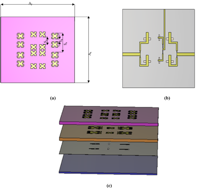
Array 1 × 2 configuration. (a) Parasitic patches only on top of 1st substrate. (b) Back of 3rd substrate Parasitic patches and driven patches. (c) 3D design of 1 × 2 array.
3D design of this array is illustrated in Fig. 11c. In Fig. 12a,b, the design achieves resonance at 9.15 GHz (X-band), with a bandwidth from 8.7 to 9.96 GHz and a gain of 6.3 dBi. At the Ku-band, the design achieves matching impedance at 16.4 GHz, with a gain of 11.4 dBi and a bandwidth from 15.9 to 16.67 GHz. Figure 12c demonstrates minimal coupling between elements.
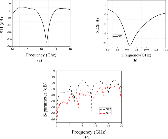
(a) Simulated result at Ku band in array 1 × 2. (b) Simulated result at X band in array 1 × 2. (c) Coupling parameters between three ports in array 1 × 2.
Array 1 × 4 configuration
Final design is done by expanding the array to a 1 × 4 configuration with total dimension L1 = 65.1 mm and W1 = 71.2 mm. A gain of 11.17 dBi is achieved at the X-band, and a gain of 14.22 dBi is obtained at the Ku-band. In Fig. 13 from figure a to figure d the final 1 × 4 array is formed by vertically repeating the 1 × 2 array with the same element spacing. The feeding network is also expanded to support the four elements. Table 1 presents the array’s parameters.
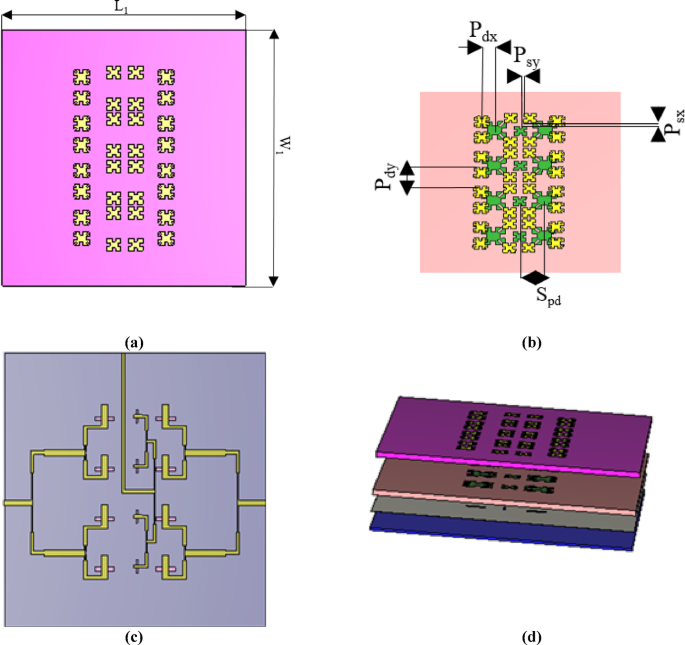
Final array configuration (a) Parasitic patches only on top of 1st substrate. (b)Parasitic patches and driven patches. (c) Back of array (d) 3D design of final array.
At the X-band, the simulated results show good matching at 10.14 GHz with a bandwidth of 0.52 GHz is shown in Fig. 14a, while at the Ku-band, the antenna operates at 16.35 GHz with a bandwidth of 0.67 GHz is shown in Fig. 14b. Good radiation pattern is achieved at X band and Ku band and are shown at Fig. 14c,d respectively.
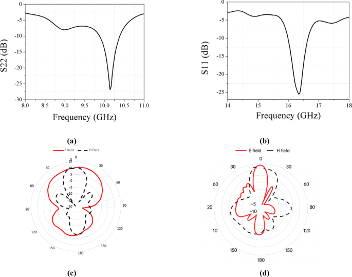
Final array configuration (a) Simulated results at X band in final array 1 × 4. (b) Simulated results at Ku band in final Array 1 × 4. (c) Simulated radiation pattern at X band in final array 1 × 4. (d) Simulated radiation pattern at Ku band in final array 1 × 4.