
Different from imaging and sensing, where interferometric scattering is initiated from randomly distributed nano-scatterers including nanoparticles, macromolecules, or local inhomogeneities in the focal volume, i-SOT resorts to the intentionally induced nanopore as an initial scatterer. It has been well established that nanopores of all dimensions less than a hundred of nanometers are created due to micro-explosion by focused femtosecond laser excitation of various transparent solids, from glassy to crystalline phases17,18,19,20,21. Because the excitation of materials at the focal point center is so strong, a high-density electron-ion plasma occurs, which then releases the deposited energy in an explosive way. This leads to complete cleavage of covalent bonds in the core volume, and thus forms core-shell-like nanopores22,23. Provided nanopores be closely arrayed, they readily produce nanometric lateral slicing plane. However, this goal is hindered by the neighboring effect, that is, new nanopores are not possibly generated near a pre-existingone since the latter tends to scatter off the incident energy so that the remaining energy becomes insufficient to produce any material damage. A reasonably large separation, e.g., several times of the initial pore size, is considered as a prerequisite for a neighboring nanopore formation. A modificative layer containing such sparsely distributed nanopores is not mechanically weak enough for femtosecond laser machining.
An unexpected phenomenon was observed when the incident laser approached a pre-formed nanopore as the initial scatterer within a critical distance, e.g., < 200 nm (Fig. 1a). The scattered light interferes coherently with the undisturbed portion of the incident beam (Fig. 1b), producing a localized intensity maximum that induces a secondary nanopore (Fig. 1b). By slightly shifting the incident laser laterally relative to an existing scatterer, secondary scatterers are consecutively generated (Fig. 1c, d). Experimentally, a 515 nm pulsed laser with a pulse width of 230 fs was focused into fused silica as the testing material through an objective lens with NA = 0.6. An 80 nm diameter spherical nanopore is produced as expected as the initial scatterers (Fig. 1e), and a 100 nm lateral offset, δ, leads to a secondary nanopore of similar shape and size (Fig. 1f). This secondary nanopore subsequently functions as a new scattering center, enabling the formation of a third nanopore (Fig. 1g), and the process proceed iteratively (Fig. 1h).
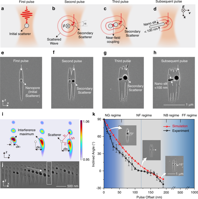
a–d Schematic production of initial and secondary scatterers. The initial scatterer, a nanopore, is purposely induced by femtosecond laser induced micro-explosion, from which the scattered light interferes with the incident light, producing a secondary scatterer. The 3rd scatter is then created by the interferometric scattering between the 2nd scatter and the incidence. The wave vector k is oriented vertically downward, the polarization direction E is perpendicular to the paper plane, and the laser spot moves to the right. e–h Scanning electron microscopic images. Evolution of the structure inside silica at a depth of 50 μm. The lateral offset is δ = 100 nm, with the wave vector, polarization, and spot movement directions consistent with the schematic. i Simulation of interferometric scattering effect from a nanopore. The initial and secondary scatterers with varied offsets of 40 nm, 140 nm, and 180 nm. The intensity in the figure is relative intensity, with the incident field intensity being 1 and the unit of color bar is 1. j An example of the nanopore propagation with a lateral offset 180 nm. k The relationship between tilt angle, α, of the secondary nanopore relative to its seed and the lateral offset
The above process is readily recognized as the interferometric scattering effect but with the nanopores instead of nanoparticles as the scatterers. The validity of the nanopores as scattering centers is then examined by a numerical electromagnetic calculation using COMSOL Multiphysics. In the core-shell-like model, the nanopores were assigned a slightly reduced refractive index relative to the surrounding matrix23, as is reasonable since the core volume consists of diluted material due to micro-explosion. When irradiated by a laser beam that is laterally offset from the scattering center, each nanopore functions as an excited electric dipole, oscillating along the polarization direction (perpendicular to the plane of the paper). The near-field component dominates the dipole radiation24 since the nanopore size is much smaller than the wavelength (< λ/10), which is then expressed as:
$${{\boldsymbol{E}}}_{sca}^{near}({\boldsymbol{r}},t)=\frac{1}{4\pi \varepsilon }\frac{3\hat{{\boldsymbol{r}}}(\hat{{\boldsymbol{r}}}\cdot {\boldsymbol{p}})-{\boldsymbol{p}}}{{r}^{3}}{e}^{i(kr-\omega t)}$$
where p = γEinc is the amplitude of the electric dipole vector, and γ is the polarizability.
The simulation confirms that scattered light does interfere constructively with the incident beam, producing a series of intensity maxima along the optical axis (Fig. 1i). The primary (0th-order) speckle exhibits a sub-diffraction limit size and an intensity up to 10% higher than the incident beam, creating favorable conditions for secondary scatterer formation via micro-explosion. The lateral offset δ determines the position of the secondary scatterers within a critical range of δ < 200 nm. Experimentally, δ = 40 nm (Fig. 1i, left), δ = 140 nm (Fig. 1i, center), and δ = 180 nm (Fig. 1i, right) all produce secondary scatterers of intervals equal to the offsets.
It is interesting to notice from the simulation that high-order interference speckles always exist, and the relative distances among the initial scatterer, 0th and high-order speckles follows a phase condition: ∆h + l2 – l1 = mλ, where m denotes interference order, λ denotes the wavelength in the medium, ∆h denotes the longitudinal height difference between the extremum points of the interference field, and l1, l2 denote the distances from the nanoseed to the extreme points respectively. Assuming three-photon absorption process, δ = 40 nm and δ = 180 nm lead to 1st order interference speckle intensity of 90.4% and 95.7% of the 0th order (Fig. 1i). If the incident laser power is purposely increased, and the offset is chosen to 180 nm, near the upper limit of the critical range, high-order interference intensity maxima, up to m = 3 are all printed to material (Fig. 1j). These results unequivocally demonstrate the role of interferometric scattering in the sub-diffraction-limit formation of secondary nanopores.
The laser beam offset, δ, plays a critical role in the secondary nanopore induction and evolution, according to which four different light-matter interaction regimes are divided (Fig. 1k). (i) Far-field (FF) regime (δ > 500 nm), defined by the lateral diffraction limit, where micro-explosion occurs insusceptible to the existence of early produced scatterers; (ii) Neighbor (NB) regime (500 nm > δ > 200 nm), where neighboring effect dominates with δ between the far-field and near-field limits. Neither secondary nor isolated nanopores can be formed due to insufficient energy deposition; (iii) Near-field (NF) regime (δ < 200 nm). Scattering interference effect dominates and secondary nanopores are deterministically generated. (iv) Nanograting (NG) regime (δ < 50 nm) as a special case of regime III. In this case, secondary nanopores are subjected to disturbance and modulation by its scatterer, resulting in a spatially overlapped volume consisteing of nanogratings. The δ values categorizing different regimes are dependent on materials, but the existence of the four regimes is universal to various transparent solids.
The near-field regime with 50 nm < δ < 200 nm works for continuous production of secondary scatterers. Once δ is chosen, the vertical coordinate, or the orientation of a secondary nanopore, defined by the inclined angle, α, is spontaneously fixed (Fig. 1b). Technically it means the convenience determining a secondary nanopore orientation simply by the offset selection. Both simulation and experiments exhibit that scanning δ from 0 to 190 nm yields a monotonic decrease in α, from 90° to -25°. There are three special cases worthy of further discussion. The first case, δ = 0 nm and α = 90° corresponds to a secondary nanopore directly above the initial seed. This configuration enables backscattering interference as previously reported25, whereby vertical nanopore arrays facilitate high-aspect-ratio dicing (>10,000:1). The second case occurs when 0 > α > -20°, achieved by 120 nm < δ < 190 nm. The occurrence of forward interferometric scattering is completely out of our expectations when the backscattering interference model was built25. This, together with the fact of tilt slicing along any angle of (δ = 50 ~ 120 nm; α = 0 ~ 30°), means the unique capability of optical nanofabrication of complex 3D geometries in transparent solids by subtractive and modificative means. In contrast, such high accuracy fabrication was achieved only by an additive approach, for example, two-photon-induced photopolymerization10,26,27,28,29. The third case is α = 0° achieved under δ = 120 nm. Sequential lateral extension of secondary nanopores is exactly the conditions required for lateral slicing, laying the foundation for i-SOT-based wafering applications.
Femtosecond laser writing by interferometric scattering effect
Femtosecond laser direct writing has been established as a powerful tool to manufacture complex 3D structures and devices for a wide variety of applications during the last decade. Despite sub-micrometer or even nanometer spatial resolution has been claimed, most of them denote lateral spatial resolution. Since any focal spot from a focusing lens takes intrinsically ellipsoid form with long axis parallel to the light beam direction, the vertical spatial resolution, although of the same importance for 3D fabrication as the lateral one, is much worse and hence less discussed. The interferometric scattering produces secondary nanopores by light maxima of more sphere shape from two-beam interference, which dramatically improves the vertical spatial resolution.
Interferometric scattering effect allows for femtosecond laser scattering writing, i.e., complex 3D shapes are created by secondary nanopores propagation instead by focal spot depicting. In this circumstance, the laser beam offset, δ, simultaneously determines x and z coordinates of secondary nanopores, with the initial nanopore serving as the coordinate origin (Fig. 1k). This enables writing of arbitrary 3D trajectories within transparent solids through precise manipulation of δ, as exemplified by the work line illustrated in polar coordinates (Fig. 2a). This holds true only within localized regions where variations in δ do not significantly alter the light intensity distribution around existing scatterers.
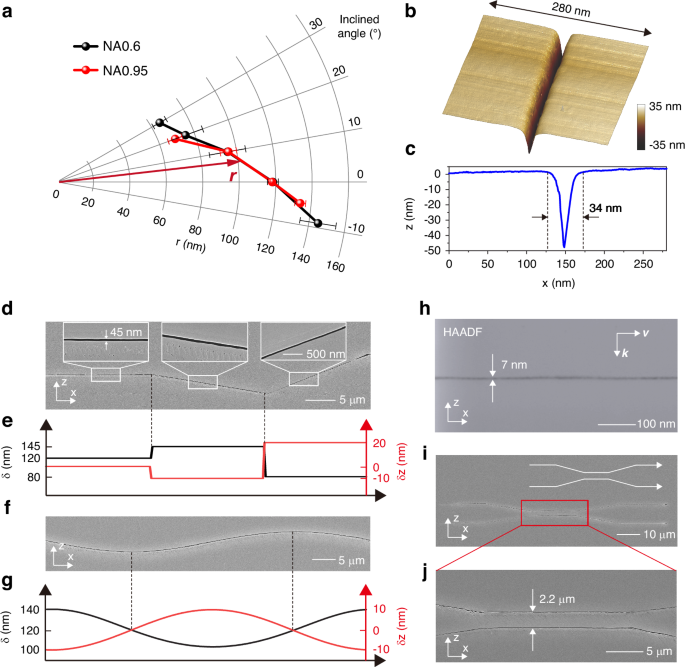
a Polar plot showing the relationship between the nano-slit orientation, α, versus the laser beam offsets. b, c Atomic Force Microscopy (AFM) images of the nanoslit after slight etching. d Three-segment zigzag nano-slit structure with 3 magnified views. e Corresponding strategy of offsets design. f Curved nano-slit structure and g the corresponding offset design. h High-angle annular dark-field (HAADF) STEM image of a horizontal nano-slit. i, j Demonstration of nearest achievable nano-slit spacing, showing the hindrance of neighboring effect
For large-scale patterning, it is essential to dynamically adjust the laser focal spot along the desired trajectory to maintain a consistent scattering interference pattern. In this process, the lateral step size δ governs the orientation, α and z-coordinate of subsequent nanopores, while the vertical step size δz ensures consistent energy delivery for stable formation of secondary nanostructures.
The determination of δz requires an iterative optimization process since elevating the focal spot alters the scattering interference conditions. It is, however, a fast convergence process both experimentally and numerically, and isn’t challenging. A parameter set of δ = 120 nm and δz = 0 nm, denoted by (120, 0) produces a lateral straight line (Fig. 2d, left, e), while (143, -25) and (75, 27) lead to tilted straight lines of incident angles of -10° (Fig. 2d, middle, e) and 20° (Fig. 2d, right, e), respectively. It is not surprising that smooth, wavy lines (Fig. 2f) are produced by laser focal spot scanning with pinpoint (δ, δz) setting (Fig. 2g). There are two points that are worth mentioning. First, a purposely chosen laser pulse energy destroys the wall between the secondary nanopore and its initial scatterer, and an internally connected inverse nanowire forms naturally following the scanning locus. 3D networks consisting of the inverse nanowires may find immediate applications in lab-on-a-chip systems, nanofluidic cooling structures for electronic and photonic chips, and biological filtering membranes. Second, the nanoscale feature is maintained after the secondary nanopore connection, as is proved by 34 nm wire width even after sample polishing and etching for atomic force microscopy (Fig. 2b, c). The smallest linewidth achieved experimentally is solely 7 nm (Fig. 2h) for the raw modified layer, which is magnified to 45 nm by wet etching for ease of SEM imaging. The minimum kerf width achieved experimentally is 7 nm in i-SOT wafering, as detailed later.
Interferometric scattering-based optical tomoslicing (i-SOT)
In simulations and experiments, we found that the aforementioned interference scattering model and nanoslit fabrication are applicable not only to a single spherical seed but also to a linear seed. We use a cylindrical lens (Fig. 3a) to produce a nanoslit, closely arrayed and inter-connected nanopores, as the initial scatterer. Surprisingly the initial nano-slit scatterer yields secondary nano-slits the same way as nanopores do. This enables a laser wire sawing tool to precisely slice a transparent solid into pieces. The ability is termed optical tomoslicing, which overcomes the limit of vertical spatial resolution by interferometric scattering, similar to the case of laser scattering writing discussed earlier. The entire technology is thus defined as i-SOT, i.e., interferometric scattering-based optical tomoslicing.
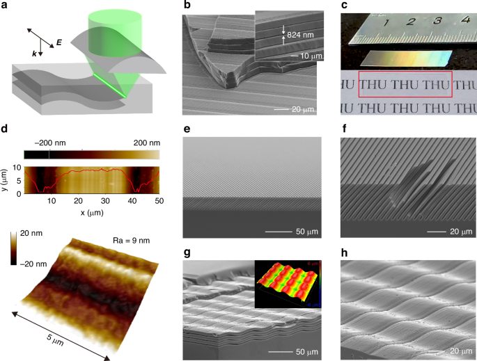
a Schematic of line light field production by a cylindrical lens. b Planar slicing results showing a kerf width of 824 nm, local and magnified views. c Planar wafering with high transmittance using cold split without etching. The wafering size is 30×10 mm. d Surface flatness of the sliced surface. The overall roughness, Ra ~ 9 nm inside a line light field, and Ra ~160 nm considering the inter-field connection. e, f Tilted slicing with an inclination angle of ~45°. g, h Demonstration of wavy slicing. The peak-to-valley height difference is 12 μm, the period is 70 μm, and the minimum radius of curvature is approximately 21 μm
The i-SOT technology defines the slicing trace by pinpoint offset setting (Fig. 2a), too, instead by direct focal line scanning. Experimentally, the 515-nm-wavelength, 230-fs-pulsewidth laser beam was focused by a cylindrical lens with a focal length of 400 mm to generate a line optical field. The beam is then compressed and projected through a 4 f beam reduction system to create a line light field at its focal plane (Fig. 3a). The first unprecedented effect of i-SOT usage is the sub-micrometer kerf width (Fig. 3b). For example, the layer space in a horizontally sliced 10-μm-thick wafer is 824 nm, which is larger than the raw kerf value since it was widened by etching for the visibility under SEM. The i-SOT technology allows direct split16 after laser process with a kerf width of only 7 nm. As seen in Fig. 3c, a 30×10 mm slice was obtained (see methods). The small kerf naturally leads to smaller surface roughness, for example, Ra = 9 nm within a line field range, and 160 nm considering the inter-field seams (Fig. 3d). Both the kerf and surface roughness are more than two orders of magnitude superior to those by conventional wafering technologies, ~20 μm by laser-assisted approach, and ~40 μm in diamond- or slurry-based wire sawing. A wafer of 100-μm thickness with a kerf of submicron width denotes mass loss less than 1%, a level reasonably called kerf-free for crystal wafering.
Another unique advantage of i-SOT is the high processing efficiency inherent in the line-form, instead of point-form light field. With a cylinder lens of NA = 0.6, the light field can be transformed to to a width of 50 μm width and scanned at1 m/s velocity, as may be lifted by further extending the line field length to, for example, 20 mm, which accounts for a scanning efficiency of 0.02 m2/s. In addition, both the thin wafer thickness and small kerf width allow for consecutive multi-layer wafering. Different tilt angle wafering has been demonstrated. As an example, Fig. 3e, f show 45° angle tilt wafering. The largest possible layer number is restrained by the lens working distance and wafer thickness. Generally, 10-μm wafer thickness is safe for neighboring plane exposure, and under extreme condition, a 2.2-μm thickness has been achieved (Fig. 2i, j). As an extension of the case in Fig. 2f, where a wavy inverse nano-slit is demonstrated, curved-surface wafers of wavy cross-sections are attained by scanning with proper (δ, δz) setting (Fig. 3g, h).
Wafering of crystalline materials by i-SOT
The i-SOT technology has been approved valid using fused silica as the test material. There is no doubt that it is applicable to other transparent solids since interferometric scattering effect is universal upon femtosecond laser excitation. However, the inherent mechanical anisotropy induces competition between two mechanisms: secondary nanopore-governed slicing and local expansion-dominated cleavage along high-index crystalline planes. The 3D regular arraying of atoms categorizes crystals into 14 symmetry point groups and 230 space groups, leading to a relatively weak connection between low-index planes, as laying the foundation for semiconductor cleavage physics. In i-SOT of crystalline materials, laser-induced micro-explosion causes local expansion around nanopores or nano-slits, which serves not only as the scattering center for the secondary nanopores and nano-slits generation, but also the seeds of cleavage along low-index planes upon shockwave actions from subsequent laser pulses. It is obvious that slicing crystals by i-SOT along low-index plane tangent direction as done in common laser-assisted wafering, jointly aided by the two forces, would much facilitate the wafering process.
Experimentally, YAG (Fig. 4a-e, h) and MgAl₂O₄ (Fig. 4f, g) crystals are processed by i-SOT along the (100) plane. In a sequential 4-layer YAG slicing of 8.6-μm wafer thickness and 0.9-μm kerf width, complete cleavage between layers is firmly approved by internal X-Ray imaging (Fig. S17d), as well as by the steplike planes of fracture in Fig.4a. The ease of spalling of i-SOT-sliced crystals is obviously observed from the random separation of the 4-layer wafers (Fig. 4g). Separated wafers allows for further processing by femtosecond laser, such as being cut into 1mm-side length square (Fig. 4b) or 0.5mm-diameter disk (Fig. 4d). 150 holes of regular 30-μm diameter are further drilled out of the YAG slab (Fig. 4c). Smaller structures of complicated geometries are also machined from the wafers of different crystals, Ce:YAG (Fig. 4e) and MgAl₂O₄ (Fig. 4f).
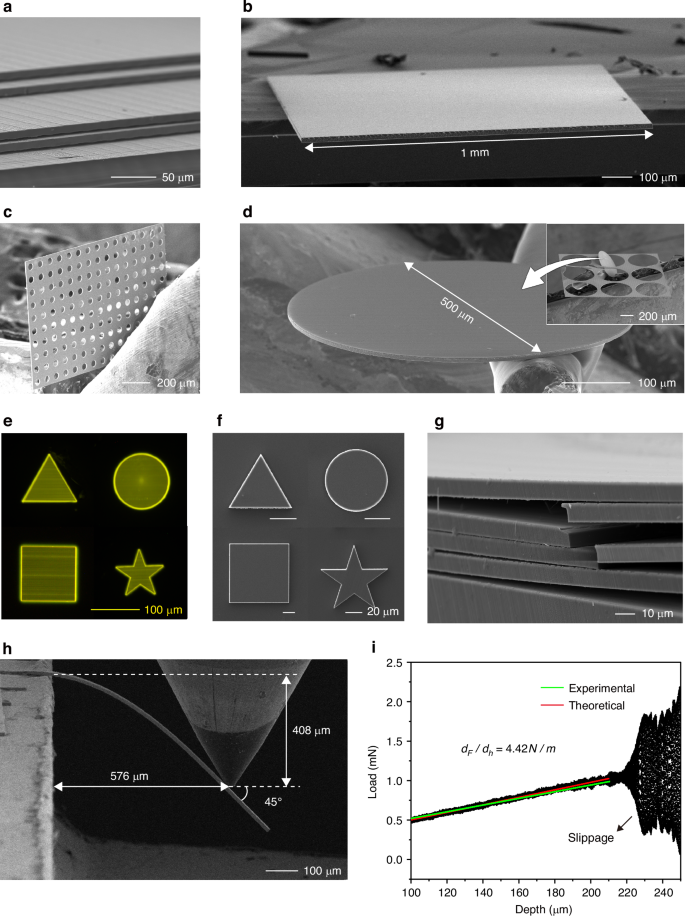
a 4-layer slicing of pure YAG crystals. The wafer thickness is 8.6 μm and the kerf width is 0.9 μm. b Square YAG thin plate with a side length of 1 mm. c Nd: YAG thin-plate with a 10×15 holes array. The diameter of the holes is 30 µm. d Disk-shaped YAG thin plate with a diameter of 500 μm. e Fluorescence images of Ce: YAG slices with sdifferent shapes. f SEM micrographs of MgAl₂O₄ crystal slices with complex shapes. g Cross-sectional view of MgAl₂O₄ slices with a thickness of 9.5 μm. h Mechanical properties test of sliced YAG thin plate. Cantilever thickness: 9.55 μm, width: 30 μm, length: 1 mm. i Corresponding stress-strain curve demonstrating the robust mechanical integrity of these ultrathin YAG plates
i-SOT wafering and subsequent laser fine machining of crystals cause negligible sub-surface and internal mechnical damage. To confirm this, a 1-mm long, 9.95-µm thick YAG slab cantilever was fabricated and subjected to a bending test with a diamond indenter. The cantilever exhibits excellent flexibility, as it reaches a maximum bending angle of 45° and a minimum radius of curvature of 271 µm before frictional slipping occurred at 220 µm displacement, causing oscillations in the force curve (Fig. 4i). The measured force-displacement slope was 4.42 N/m, closely matching the theoretical value of 4.24 N/m calculated from YAG’s Young’s modulus. No mechanical fatigue or performance degradation was detected after aging tests.