Key Takeaways:
- Flexible ICs are durable and form-fitting, but they add manufacturing challenges to already complex processes, while printed flex sensors lack infrastructure.
- MEMS are finding new popularity in massively parallel systems, on one device, or in many devices distributed across a network.
- Metal oxide-based sensors are more scalable than those relying on photonic crystals, because metal oxides are not spoiled by humidity.
Today’s digital technology, loaded with artificial intelligence and machine learning, is being harnessed to get closer readings on analog real-world data from the environment and the human body.
The latest sensor technology can mimic nature while AI/ML enables distributed intelligence and real-time analysis. To achieve this, established technologies are being deployed in increasingly complex applications that require innovative manufacturing and chemistry techniques.
Examples of established technology in new sensor and medtech devices:
- Flexible ICs: The idea has been around for up to a century, but now they are being bent into 3D packages. The conducting paths of the circuit are built on a flexible plastic substrate, usually made of polyimide, PEEK, or polyester, and the components are soldered to exposed copper pads.
- Flexible hybrid electronics (FHE): A newer solution that combines the advantages of printed electronics, such as conductive inks and stretchability, with advanced, high-performance CMOS-based silicon components.
- Microelectromechanical systems (MEMS): Originating in the 1960s, new higher-fidelity devices are being used in array transducers in medical devices and more.
- Semiconducting metal oxides: Long known to have excellent sensing capabilities, these are being used in olfactory sensors to mimic biological abilities.
Flexible sensors and devices
Demand for flexible is growing across a variety of applications, including consumer wearables, implantable medical devices, soft robotics, foldable phones, stretchy displays, environmental sensors, and smart packaging of goods.
“Traditionally, devices have been on rigid substrates — a ceramic substrate, an organic kind of PC board, or a metal substrate for an RF device,” said David Fromm, COO at Promex. “There are a lot of advantages to using flexible electronics. They’re durable, they’re form-fitting, and you can fold them up to take advantage of that three-dimensional package.”
The downside is that flexible substrates need custom processes to deal with all the complications that crop up to ensure high yield and high, Fromm explained. “The problems are additive, and typically not even linearly additive in terms of the complication. Everybody wants to do everything. It’s a matter of keeping that complication, because that provides the benefits.”
Over the next five years, the ratio of rigid substrates to flexible substrates is expected to level out to just about even. “The name of the game is integration, and being able to service the full stack of offerings coming in from raw materials all the way to finished product, whatever those might be,” he said. “Those could be wafers for people handling bare die. They could be surface-mount components on tape and reel. The finished product is a thing on a flex that could be mounted into some other box or housing.”
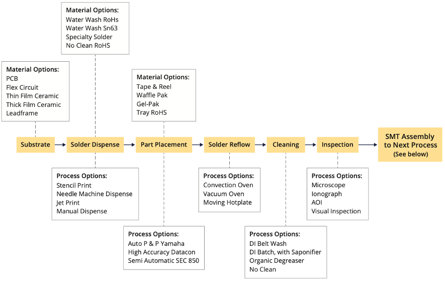
Fig. 1: Sub-assembly using surface mount technology (SMT) process. Source: Promex
Advanced packaging innovation varies by customer, and how willing they are to experiment. “I’ve put die products in all kinds of crazy places in my career,” said John Weil, vice president and general manager for IoT and edge AI processors at Synaptics. “I’ve even seen people back-grind it so thin that it’s actually considered flexible. When you move to these advanced process nodes, you lose some of that flexibility, no pun intended. But it comes down to a packaging exercise. Our latest edge AI MCU is an organic substrate with a flip-chip die product. It’s not huge, but you’re not going to mount it on the tip of a pen. The technology is capable of getting that small, but that would be a different product.”
Many companies are still figuring out what to do with flexible ICs. “A lot of these projects are at a university level, research level, where you’re trying to understand how they would integrate into real-life environments,” said Hariharan Mani, semiconductor applications engineering leader at Infineon Technologies. “So far, our focus there is more on the research side. We don’t have an end product that is in the flexible sensor category. We have been focusing more on environmentally oriented sensors. A lot of our sensors have access to the environment. Usually, they have a port on the sensor itself, so a microphone or a pressure sensor that is looking outward into the environment and trying to convert it digitally.”
Flexible MEMS
Many ICs in the consumer space and various vertical markets include MEMS sensors and/or actuators, whether on a flexible or rigid substrate. The technology has been around for decades, but the trend is toward higher-fidelity devices, so they do more.
“You can get a richness of data,” said Fromm. “It might be that instead of getting a single point sensing, you get an image of sensing across a wide array.
For example, Promex is working on a MEMS array transducer. “There are many, many transducers in an array,” he said. “Each of those requires a lot of computing power to form, say, an image from this array of transducer elements at high speeds with low noise and low power consumption. That’s a typical use case for a MEMS device. It could be a medical or consumer device, or anything. Attaching this transducer element, with high yield so that all the pixels are active, is challenging. Then the high computing power creates a lot of issues.”
Customers are looking to use MEMS in massively parallel systems. “This could be parallel on one device, or making many devices and distributing them across the network of where these things go,” said Fromm. “To make this happen, many MEMS go on to flexible substrates, and the complications are, ‘How do you ensure all of the connections are made properly, and that they’re made durable enough to meet the life cycle demands of that device on a flexible piece of polyimide?’ That’s hard to do.”
Promex built one customer’s MEMs array transducer on high-density flip chip, which is challenging enough on a typical organic substrate. “Doing it on a flex is very difficult to do with high yield,” said Fromm. “The other issue is that they impact the design. You typically think of laying out a circuit board as an electrical engineering problem. I’ve got to route the signals, and then the power, and keep them separated so that there’s no noise issues or whatever. This is all true on a flex. But now, think about the mechanical issues associated with that assembly. In the flip chip processes, I’m doing solder reflow and there are stresses on those parts due to the coefficient of thermal expansion, mismatches, and so forth. You can break the traces inside the flex.”
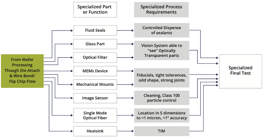
Fig. 2: Specialized part placement and attach. Source: Promex
Reliability and simulation challenges
In terms of reliability, most of the issues on flexible devices are below them or around them on the flex, not on the interconnects or the solder joints.
“When you lay out the traces, which is the thickness and the planar dimensions of the traces and pads, you have to consider where the weak points mechanically are, which oftentimes you don’t know until you build it,” Fromm said. “You see things are breaking, and you fix it, or you build it and it survives. It goes out in the field, and then during use, you see you’ve got problems that need to be fixed. That’s a really complicated thing, oftentimes very difficult to simulate. There may not be best practices for your device because your geometry is different than some other devices. Geometry is the biggest challenge of these high-tech, high-smarts flexible devices. Is the mechanical rigidity, and stability of those devices to make them, durable and reliable enough to become a real product?”
Designers typically use the Von Mises stress value — rather than the fundamental physical component stress method — to determine if a given material will yield or fracture due to displacement and stress. “It’s not just how much, but also in which direction the displacement is,” said Marc Swinnen, director of product marketing at Synopsys. “You have x,y,z stresses, and then you have torque rotational stresses in three axes. There’s normally, in every material element, six possible vectors of stress. It’s totally impractical to analyze that across the shape, so Von Mises stresses are a way of mathematically reducing that complexity down to a single number that is meaningful and actionable.”
Stress vectors have added implications for flexible ICs. “Because stress and displacement are sort of two sides of the same coin, if you make something flexible, it will relieve stresses by bending, so the stresses will be low, but the displacement will be high,” said Swinnen. “But if you make it stiff and rigid, the displacement will be minimized, but the stresses will build up. You would need to find a medium there, and that is definitely being done. TSMC and others are very concerned about thermomechanical deformations, and this hits reliability downstream. We know of production projects from big companies that have failed in the field, and it was all due to thermomechanical stresses breaking the contacts. All the units had to be recalled. Thermo-mechanical reliability is definitely being analyzed, and relatively early.”
However, with a brand new type of device, there will not be a lot of available data to enable a shift left methodology through simulation, allowing designers to fix problems earlier in the flow. “It’s hard,” said Fromm. “The only way you get smarter is to figure out what the rules of thumb are, which we’re all still learning, then start zeroing in on those as best practices. You have to look at the whole device as a system, which is a combination of things that we can do while manufacturing it. Ultimately, the design agent of this device needs to create an infrastructure to really drill down into those failures, to be able to measure them so that you know what’s breaking, and to test for them so that you can drive the failures and shut them down. That’s a whole different bucket of activity for product development and manufacturing process development that you wouldn’t see as often for a rigid device.”
Printed flex developments
Brewer Science has developed printed, flexible water sensors, as small as 1mm, that enable in-situ detection of contaminants such as lead. The project began in the mid-2000s with experiments into functionalizing carbon nanotubes and eventually the team figured out how to turn them into sensors.
“That’s where our sensor business really took off,” said Adam Scotch, R&D director for Smart Devices at Brewer Science. “We started developing sensors that monitor our environment — gas sensors, humidity sensors, things like that. There was a big push in flexible printed electronics, in flexible sensors. We were developing inks. Nobody could print them. We had to develop our own printing capabilities to show others how it’s done. We did that, and then we recognized that making and selling sensors wasn’t that easy. It was hard for people to take your sensor and apply it to their application, so we started developing our own devices, our own hardware.”
The company has gone through a lot of iterations, and its water sensors are no longer based on carbon nanotubes. To make them inexpensive enough, they have to be mass manufactured effectively.
“That means they have to be put down or printed in a way that’s cost-effective,” Scotch explained. “We’ve taken our knowledge in material science, in polymers and chemistry — that’s where our core knowledge base is — and figured out how that translates from our core business in semiconductors to where we are today? It’s the chemistry of the sensors itself, and then putting down this material. We had to develop printing techniques for putting this material down. These aren’t silicon chips. These are polymer-based materials, membranes with electrodes. This is as far away from silicon as you can be right now, but we’re using some of the same base materials in our sensors that we have developed over 40 years. There’s still a need for substrate materials and encapsulants that have to tolerate all kinds of water. We have to protect these materials, these sensors, over six months, from dirt and algae and anything that’s in the rainwater flowing into the water supply.”
Many companies have dabbled in printed electronics, but now it’s becoming a viable option for mass production. “It’s been a small effort for a very long time,” said Scotch. “It’s always been the future. For 20 years, 30 years, it’s gone through a series of different names.”
The main problem with printed electronics is infrastructure. “There’s no real good infrastructure in place for printed electronics, because there are thousands and thousands of applications,” he said. “Everybody rushed into printed electronics for roll-to-roll, because they thought roll-to-roll was the future. That was the way to get costs down. That’s where RFID started. That’s where all the solar stuff started. They thought, ‘The way to get costs down for everything is print it and go roll-to-roll.’ There was an infrastructure built for roll-to-roll, but the economics are that you don’t go roll-to-roll until you’re ready to make billions and billions of parts. There is very little infrastructure in place to make tens of thousands of pieces.”
Further, the metallization side has always been a problem. “For years they’ve developed conductive inks,” said Scotch. “Conductive inks are mostly silver-based, and the printed inks have very, very high resistance. This is a problem because if you’re trying to make a sensor and half of your power is being taken up by your traces, it’s never going to work long term.”
Metal oxide sensors
Harvard University researchers have been working on olfactory sensors that can sniff using a series of tiny fans on the IC, offering similar benefits to the way users can change the focus of a camera, even with the same hardware.
The devices include a photonic crystal sensor, but the team discovered that photonic crystals are not always scalable into the world. “They are spoiled by humidity,” said Haritosh Patel, a graduate student at Harvard University’s School of Engineering and Applied Sciences. “It’s a huge interference that can cause damage to the actual sensor and the readouts of it, and also to some sophisticated spectrometers to read out the readings.”
To enable real-world use cases — such as a simple food spoilage application where the metabolism of the bacteria growth can tell you how spoiled the food is, or the indoor toxins in the air people breathe — the team had to shift their perspective regarding the hardware.
“We realized that metal oxide semiconductors are ubiquitously already used as chemiresistive sensors for volatile organic compound detection and light detection,” said Patel. “Breathalyzers, sometimes even alcohol sensors, use these types of metal oxide sensors, where a simple reversible oxidation reaction to the chemiresistive surface changes and modulates resistance based on the relative presence of concentrations of different compounds.”
Harvard’s olfactory sensor leverages findings from a 1982 paper by Persaud et al., which introduced the concept of an e-nose, composed of more than one element. “The downside to a single metal oxide element was the non-selectivity of it,” explained Patel. “If we had one single non-metal oxide cell element, you wouldn’t be able to tell if the oxidative, reversible reaction was caused by one species or another, because it’s simply looking at the oxidation of it. Something twice in concentration that can oxidize might be giving a similar response in resistance to something that’s a weaker oxidizer, but in a more abundant concentration.”
Persaud’s paper showed that if engineers take multiple metal oxide elements, each doped slightly differently with a different metal oxide sensitivity, it approximately represents how we have olfactory receptors, Patel noted.
Olfactory receptors aren’t a lock-and-key mechanism. “It’s more or less that they are non-selective,” said Patel. “Even our biological olfactory receptors have select, non-specific binding, and the strength of the binding is what releases the information, rather than just a single receptor binding to a single analyte. So if we arrayed a system, let’s say 10 or 20, or even if we can go bigger systems — hundreds of metal oxide sensors all slightly doped differently — the response curves would be generated in a way where you can deconvolute what is the species that is causing the oxidation, or what is the presence of the chemicals. That was really one of our shifts.”
As soon as the team made this shift, they developed the hardware. “It was now an e-nose, created by a set of metal oxide sensors, but specifically with an addition of printed circuit board circuitry that helps that for different applications.”

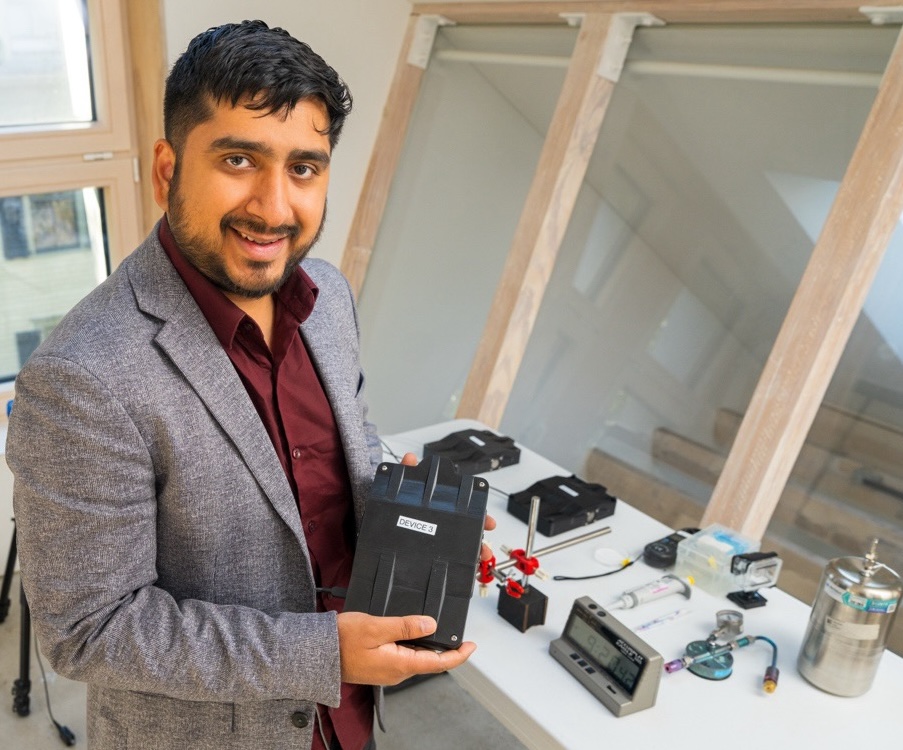
Fig. 3: Haritosh Patel with an olfactory sensor device. Source: Harvard University. Photo Credit: Wyss Institute
For certain applications developed for indoor air quality, environmental sensors would be used as well, such as temperature-humidity sensors and flow-rate sensors to help calibrate what response changes would be happening to the metal-oxide sensors, Patel said.
“Finally, when we moved past the hardware stages, we moved into some machine learning models, where there were these response curves. Different compounds, different chemicals, data sets were collected and trained in broad environmental conditions in which we can now detect concentrations down to 40 parts per billion, if not even lower, for formaldehyde in an indoor system like this, with relatively cheap off-the-shelf commercial metal oxide sensors,” explained Patel. “It’s more like using surface mount devices in the right combination with machine learning algorithms that achieves the final goal of chemical detection.”
Conclusion
The latest developments in sensors and ICs are proof that established technology can find new life in leading-edge applications. For example, previous ideas around flexible ICs centered on industrial operations, measuring flow on valves and things like that in an ad hoc setup. Printed, flexible sensors to measure data in real time offer a complete change.
The challenge is to take technology — including the sensors and the materials — and enable it to be translated across disciplines. “There’s all the other ancillary stuff that nobody really talks about, and that’s, ‘How do you put down that material?’” said Brewer Science’s Scotch. “How long will it last? What substrate do you put it on? What other materials are necessary?”
There’s not a lot of these devices on the market right now, but a lot of need. “A lot of small startups and universities are trying to develop technologies to be able to do these things,” Scotch said. “It will come, and there’s enough room for many, many players because there are so many applications to dig into.”
Related Reading
Environmental Sensors Catch More Data For A Greener World
New types of sensors can generate environmental data in real time using a range of tools, including flexible, printed ICs and AI/ML.
Precision Under Pressure: Managing Materials Complexity In Advanced Packaging
As packaging integrates diverse substrates, adhesives, and exotic metals, manufacturers must rethink precision from the ground up.
Advanced Packaging Depends On Materials And Co-Design
New materials play a pivotal role, but solving integration problems remains a challenge.
Upcoming Challenges And Changes In Semiconductor Materials
Brewer Science’s new co-CEOs talk about shifts in materials for IC manufacturing, flexible substrates, and the uncertainties in advanced packaging.