
gettyimages.com
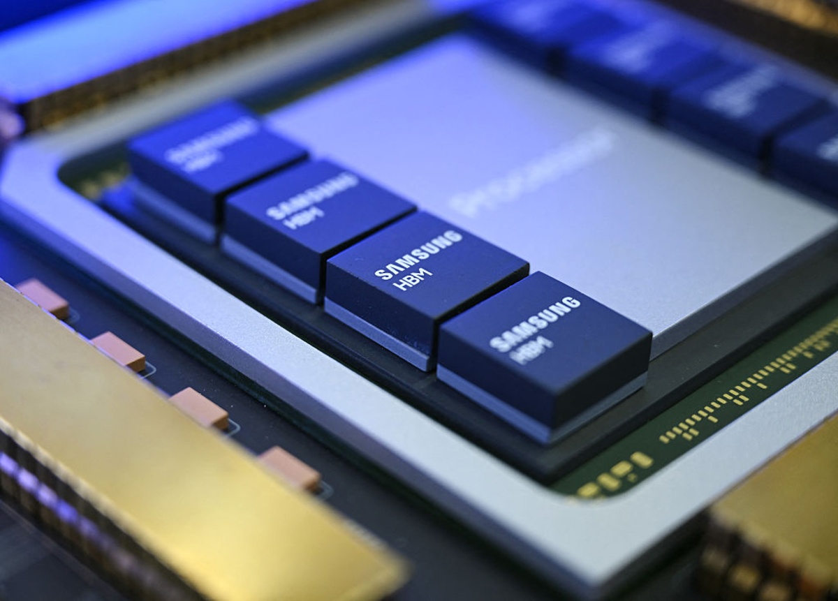
Samsung Electronics took the stage at the Future of Memory and Storage (FMS) 2026 conference in Santa Clara on Tuesday and introduced two technologies that together stake out the company’s most ambitious architectural positions in memory’s history: BV-NAND, a prototype that breaks the 400-layer barrier in NAND flash by separating the manufacturing of memory cells from their control circuitry, and zHBM, a concept in which high-bandwidth memory is stacked vertically atop an AI accelerator die rather than placed beside it — making the silicon interposer that has underpinned every HBM generation to date structurally optional for the first time.
The disclosures, made at the conference’s 20th anniversary edition and reported Tuesday by Reuters, represent distinct but related bets: BV-NAND is a near-term commercial proposition, with Samsung indicating production is on the near-term horizon; zHBM is a longer-horizon architectural concept whose performance targets, if realized, would redefine how AI accelerators relate to their memory systems.
The commercial stakes are high. Every AI inference query requires retrieving model weights, context, and intermediate computation states from storage — placing high-density NAND flash in the critical path of AI system performance. As AI workloads expand from training large language models toward continuous inference at scale, that demand has intensified considerably.
What BV-NAND’s Wafer-Bonding Architecture Actually Does Differently
The difficulty of stacking NAND memory cells beyond approximately 300 layers has been a structural constraint in the industry for several years, and it comes down to a manufacturing sequence problem. In the conventional Cell-on-Peripheral (COP) design that has dominated NAND production since SK Hynix introduced the architecture in 2018, the peripheral control circuitry — the transistors that govern reading, writing, and erasing data — is fabricated beneath the memory cell array on the same wafer. That arrangement minimizes chip area, but it creates a conflict: manufacturing memory cells at high layer counts requires high-temperature etching processes that degrade peripheral transistors beneath the array.
Samsung’s V10 Bonding V-NAND, or BV-NAND, resolves this by building the memory cell array on one wafer and the peripheral circuit on a separate wafer using a process node optimized for high-performance logic — then bonding the two together at the wafer level. Neither structure experiences the other’s thermal environment during fabrication. The cell array wafer can be etched as deep as the process allows without concern for damaging the logic layer; the logic wafer can use process nodes that would otherwise be incompatible with the cell fabrication temperatures. The result, Samsung says, is a 58% increase in memory density compared to its ninth-generation V9 NAND, with improvements to read speed, write speed, and input/output throughput tuned specifically for AI inference workloads.
Samsung calls BV-NAND the “dream NAND for AI,” a positioning the company has been building toward since the V10 roadmap appeared in Korean trade press in late 2024. BV-NAND is not the first wafer-bonded NAND: Kioxia’s equivalent, which the Japanese manufacturer calls CMOS-Bonded-to-Array, anchors the BiCS10 generation at 332 layers — the foundation of the Kioxia CM10 enterprise SSD also debuted at FMS 2026. Samsung’s version, at more than 400 layers, claims a density advantage on top of the architectural advantage.
zHBM: What Changes When Memory Moves Above the Chip
Samsung also presented concept models Tuesday for what it described as the industry’s first zHBM — “zero-distance” High Bandwidth Memory — and a companion technology called zNAND-O.
In every HBM generation from HBM1 through the HBM5 currently targeting 2028 mass production, memory stacks are positioned laterally beside the AI accelerator on a silicon interposer — a substrate embedded with fine copper wiring that carries data horizontally between the processor die and the memory stacks. The interposer arrangement is what makes HBM fast: it eliminates the centimeter-scale distance of board-level memory routing and replaces it with micrometer-scale connections. But the interposer itself still imposes a horizontal data path that adds latency and energy cost.
Samsung’s zHBM eliminates that horizontal path by stacking HBM directly above the AI accelerator die, with through-silicon via connections running vertically between the two. Data travels straight up and down rather than across the interposer. Samsung says this achieves more than ten times HBM5’s memory density, triples energy efficiency relative to HBM5, and cuts thermal resistance by more than half.
Samsung’s CTO Song Jae-hyuk first quantified zHBM at SEMICON Korea in February 2026, stating that the technology delivers four times HBM4’s speed while consuming one quarter of the power. Applying that 4x multiplier to the JEDEC HBM4 standard maximum bandwidth of 2 terabytes per second per stack, zHBM’s theoretical bandwidth calculates to approximately 8 terabytes per second per stack.
What zHBM does not yet have is a commercial timeline. Samsung’s own HBM5 prototype debuted at Computex 2026 in May, with mass production targeted around 2028; zHBM represents a generation beyond that. The engineering challenges are substantial: a heat-generating AI accelerator die directly bonded to HBM stacks creates a thermal environment that current packaging technology has not resolved at commercial scale. Whether Samsung can achieve acceptable yield at that level of integration remains undemonstrated.
What Eliminating the Interposer Would Actually Mean
The interposer is not a passive substrate — it is the physical and commercial foundation of the current AI accelerator packaging supply chain. Every Nvidia Vera Rubin platform, every AI accelerator shipping with HBM4, depends on silicon interposers to assemble the memory-processor stack. TSMC’s CoWoS (Chip on Wafer on Substrate) advanced packaging capability is one of the most capacity-constrained elements in the entire AI supply chain, with lead times stretching beyond twelve months.
If zHBM succeeds at commercial scale, it renders that substrate unnecessary for the memory-to-accelerator connection. This would be the single largest structural implication of Samsung’s FMS 2026 announcement — not a performance claim, but a packaging-supply-chain consequence. A reader tracking only the bandwidth numbers misses the structural bet Samsung is making about where AI chip assembly economics go in the post-HBM5 era.
Samsung is not the only company pressing on this boundary. At the same FMS 2026 conference, SK Hynix announced a different architectural bet: High Bandwidth Flash, a new memory tier between HBM and SSDs developed jointly with SanDisk under an Open Compute Project standard, promising high-speed data transfer with NAND-level capacity. SK Hynix’s EVP Kim Chun-sung presented the HBF specification on Tuesday alongside a tiered memory architecture called IMTE, which adds CXL hybrid memory to extend the HBM→DRAM→SSD hierarchy and claims a 35.7% improvement in AI inference efficiency versus conventional designs, according to TrendForce. The architectural divergence — Samsung betting on zero-distance vertical integration, SK Hynix betting on tiered memory expansion — is FMS 2026’s most consequential competitive dynamic.
Does a Bigger Bet on AI Leave Less for Everyone Else?
The FMS announcement was flanked by a supply-side disclosure that carries direct implications for any buyer outside Samsung’s top-tier AI datacenter relationships.
On its Q2 2026 earnings call on July 30, Samsung disclosed that long-term supply agreements could eventually account for 60 to 70 percent of its memory sales — a structural commitment to AI datacenter customers that locks the vast majority of the company’s output into multi-year forward contracts with price floors and substantial advance payments. Samsung confirmed that five major global datacenter operators have already signed such agreements, with negotiations near completion for five additional large-scale AI customers.
The arithmetic consequence for everyone else is straightforward: if 60 to 70 percent of Samsung’s memory production is reserved for AI datacenter LTA customers, the remaining 30 to 40 percent must serve all other buyers — smartphone manufacturers, PC original equipment manufacturers, enterprise storage buyers, and the broader consumer electronics market. Samsung’s Q2 2026 results documented the same dynamic internally: its Device Solutions semiconductor division posted an all-time record profit of ₩89.2 trillion (approximately $62.5 billion) while its Galaxy mobile division — which buys commodity DRAM and NAND as inputs — posted its first-ever operating loss of ₩0.7 trillion (approximately $490 million), both consequences of memory capacity being priced and allocated toward AI at the expense of everything else.
Industry analysts project the global HBM market at approximately $58 to $60 billion in 2026, up from roughly $35 to $38 billion in 2025, as AI server deployments continue to absorb available high-bandwidth memory supply. Counterpoint Research’s Q2 2026 data placed Samsung’s overall DRAM market share at 39 percent, highest in two years — while SK Hynix maintained its lead in the HBM-specific market, with Micron expanding aggressively in both HBM and conventional DRAM.
What Samsung’s NAND Roadmap Looks Like From Here
BV-NAND is the V10 generation of Samsung’s V-NAND line. It does not arrive alone: Samsung separately disclosed earlier this year a 900-layer prototype built by bonding two 450-layer structures using a technique it calls Cell Multi-Bonding. The company’s CTO has described a “multi-BV” NAND architecture using four bonded wafers as the path toward a 1,000-layer device by 2030.
The FMS 2026 announcements position BV-NAND as the production bridge between Samsung’s current V9 NAND (in mass production at the company’s PM1763 enterprise SSD, which entered mass production July 8) and that multi-BV future. The zHBM concept, meanwhile, positions Samsung’s wafer-bonding capabilities not just as a NAND story but as the architectural mechanism for the next era of memory-processor integration — one in which the memory is not next to the chip but on top of it.
FMS 2026 runs through August 6 at the Santa Clara Convention Center, approximately 37 miles (60 kilometers) south of San Francisco, with additional keynotes from SK Hynix, Micron, Nvidia, and Kioxia scheduled for the remaining two days.
Frequently Asked QuestionsWhat is Samsung’s zHBM, and how is it different from conventional high-bandwidth memory?
All current HBM generations — from HBM1 through the upcoming HBM5 — place memory stacks beside the AI accelerator on a silicon interposer, with data traveling horizontally between the processor and the memory. Samsung’s zHBM concept places HBM stacks directly above the AI accelerator die, connected by through-silicon vias running vertically rather than horizontal interposer traces. This eliminates the horizontal data path entirely. Samsung claims the architecture achieves more than ten times HBM5 density, three times the energy efficiency, and more than a 50 percent reduction in thermal resistance — though it currently exists only as concept models with no commercial timeline disclosed.
Why does zHBM’s vertical stacking matter beyond the performance numbers?
The silicon interposer that connects HBM to AI accelerators in all current designs is one of the most constrained components in the AI chip supply chain, with advanced packaging lead times exceeding twelve months. If zHBM proves viable at commercial scale, it would make that interposer structurally unnecessary for memory-to-accelerator connections — disrupting the packaging economics that currently govern AI chip production capacity, including TSMC’s CoWoS process. That supply chain consequence is the implication that extends farthest beyond Samsung’s own performance claims.
What does the 60-70% long-term supply agreement mean for buyers outside the AI datacenter market?
If Samsung reserves 60 to 70 percent of its total future memory production for AI datacenter customers under long-term contracts, the remaining 30 to 40 percent must supply everyone else: smartphone makers, PC manufacturers, consumer electronics companies, and enterprise storage buyers. Samsung’s own Galaxy division experienced this dynamic in Q2 2026, posting its first-ever operating loss of ₩0.7 trillion (approximately $490 million) partly because elevated memory component costs — driven by the same AI supercycle that made the DS semiconductor division record-profitable in Q2 2026 — could not be passed through to Galaxy buyers.
How does Samsung’s architectural bet at FMS 2026 differ from SK Hynix’s approach?
Samsung is betting on zero-distance vertical integration: zHBM eliminates the interposer by stacking memory above the chip; BV-NAND eliminates the COP thermal ceiling by separating cell array and peripheral circuit onto different wafers. SK Hynix is betting on tiered memory expansion: its High Bandwidth Flash (HBF) technology, standardized at FMS 2026 with SanDisk under an Open Compute Project framework, adds a new memory tier between HBM and SSDs that achieves high bandwidth at NAND capacity scales. Both companies are attempting to solve the same problem — AI inference needs more memory closer to the compute — by reaching it from opposite architectural directions.