Enhanced friction with increasing electron energy dissipation rate
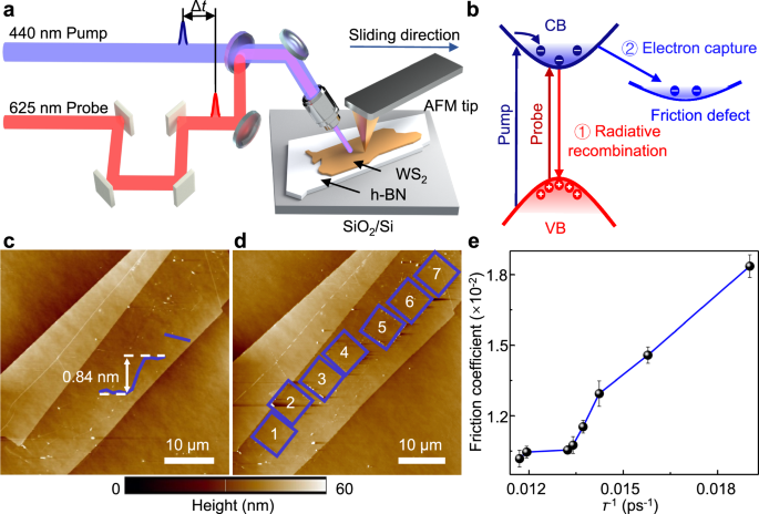
To investigate electronic friction at the sliding interface, a WS2 film-based sliding interface is established. Its exceptional electronic properties28,29 and ultra-low friction performance1,13 make WS2 an excellent platform for studying electronic friction. Figure 1c shows a topography image of a monolayer WS2 mechanically exfoliated from a bulk crystal and transferred onto a SiO2/Si substrate, with its thickness measured to be 0.84 nm via atomic force microscopy (AFM). The monolayer region is outlined with a blue dashed contour in the optical microscopy image (Supplementary Fig. 1). A multilayer of hexagonal boron nitride is encapsulated beneath the WS2 to provides a flat substrate for the sample30,31,32,33. Another component of the sliding interface is a tip with a high elastic stiffness, which slides on the sample surface using the contact mode AFM. The topography image of the sample after sliding under seven different loads is presented in Fig. 1d. The measurements reveal that there is no obvious topography change in the sliding regions.
To investigate the changes in friction properties at the sliding interface, we established the correlation between the friction coefficient and the electron energy dissipation rate, as presented in Fig. 1e. Although the surface topography of the sample shows no significant alterations following tip sliding, both the friction coefficient and the electron energy dissipation rate exhibit notable variations across seven load regions. Specifically, a clear dependence of the friction coefficient on energy dissipation rate is observed. As the sliding load increases from 100 nN to 3000 nN, the electron energy dissipation rate accelerates, while the friction coefficient exhibits a significant rise. It indicates that the increase in friction is accompanied by a higher electron energy dissipation rate. Considering the close relationship between the electronic properties of monolayer WS2 and its crystalline structure, we hypothesize that the phenomenon is closely related to the microscopic structural changes induced during the sliding process.
The measured friction force maps presents that no obvious microscopic structural changes induced by sliding are observed. To minimize the impact of adsorbate accumulation on friction, we focused analysis on the friction force signals obtained during tip sliding. Some studies suggest that friction force measurements may offer greater resolution in detecting microstructural variations compared to topography maps34,35. The friction force maps under seven sliding loads are shown in Supplementary Fig. 2, revealing no significant microscopic structural changes on the sample surface, such as wrinkles or defects. And the friction force is uniformly distributed across the entire sliding area. It suggests that these factors do not contribute to the increased friction observed in the experiment. To further elucidate the relationship between increased friction and electron behavior, it is essential to examine the more subtle microscopic changes induced by the sliding tip.
Friction enhancement caused by atomic defects
To explore the subtle microscopic structural differences after tip sliding, scanning transmission electron microscopy (STEM) tests are performed to image the atomic structure. Figure 2a presents high-angle annular dark field STEM images of monolayer WS2. A notable number of sulfur vacancies are observed in the sliding regions, which are marked by yellow circles. It is in agreement with previous reports concerning the defect distribution in monolayer WS236,37,38. Comparative analysis of atomic scale images across different sliding load conditions reveals a notable increase in defect density, rising from 0.09 nm−2 to 0.51 nm−2 as the sliding load increased (shown in Supplementary Movie). This observation aligns with other studies of TMDC materials38,39,40, indicating a strong correlation between the generation of sulfur vacancies and the applied load during sliding. Thus, the results clearly demonstrate that atomic defects are introduced on the sample surface during sliding, which can provide a new electron energy dissipation channel.
Fig. 2: Friction enhancement caused by atomic defects.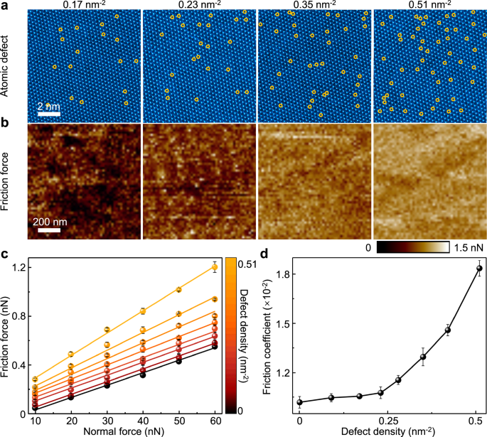
a High-angle annular dark field (HAADF) STEM images of monolayer WS2 after tip sliding. Sulfur vacancies are marked by yellow circles. The sliding loads are 500, 1000, 2000, and 3000 nN respectively. b Corresponding friction force maps under a constant normal force of 50 nN. c Relationship curve between friction force and normal force of monolayer WS2 in varying defect densities. Error bars represent the standard deviation of the data based on 256 data points. d Friction coefficient diagram under different defect densities is calculated from the line slope in c. The error bar is obtained by linearly fitting the friction coefficient. Source data of c and d is provided as a Source Data file.
To investigate the variations in friction forces across monolayer WS2 with different defect densities, we employ the lateral force module of atomic force microscopy. The friction force is measured under small normal force using a tip with a lower elastic stiffness, so defects generated during this process can be negligible. The friction force maps obtained under a constant normal force of 50 nN are presented in Fig. 2b, which compares the friction forces in regions with varying defect densities under identical testing conditions. Notably, as the defect density increases, a gradual rise in friction force is observed, consistent with trends reported in other studies of disordered materials41,42,43. The phenomenon is typically attributed to factors such as substrate roughness44 and puckering effects12,42. However, there is no disorder observed in the friction force maps shown in Fig. 2b, including phenomena such as wrinkles, wear, or localized increases in friction at defect edges. It presents that the increased friction in our experiment is not primarily driven by disorder-related mechanisms, like substrate roughness or out-of-plane deformation. And we mainly focus on the impact of atomic-level defects at the sliding interface on friction.
To further quantify the frictional properties of defective WS2 monolayer, the friction coefficients of varying defect density regions are measured. The normal forces are selected ranged from 10 to 60 nN, encompassing six distinct levels. The relationship between friction force and normal force is illustrated in Fig. 2c, where the dependence of friction on load is linear within the range of load, allowing the determination of the friction coefficient17,45. And the lateral force traces and topography of defective WS2 monolayer are shown in Supplementary Fig. 3. Consequently, the friction coefficients of monolayer WS2 are obtained to be approximately 10−2, which aligns with results from other studies on monolayer TMDC materials10,46. It also clearly indicates that monolayer WS2 exhibits excellent properties as a solid lubricant. Moreover, as the defect density increased, the friction coefficients enhanced from 0.0102 for the pristine sample to 0.0184, as shown in Fig. 2d. The lateral force traces for defective samples with different defect densities are shown in Supplementary Fig. 4. Frictional characteristics studied by atomic force microscopy demonstrate that the friction coefficients of defective WS2 nearly doubled, which is attributed to atomic-level defects caused by a sliding tip.
Evidence of electrons captured by friction defects
To obtain evidence of electrons captured by defects, we conduct Raman spectroscopy to demonstrate that atomic-level defects disrupt the periodic lattice structure of monolayer WS2, altering its electronic properties. Figure 3a illustrates the evolution of the Raman spectra as the defect density increases, with the A1g peak appearing at approximately 417 cm−1. At lower defect densities, the measured A1g peak shows no significant changes, and the spectra are well-fitted with single-peak Lorentzian curves. When the defect density is relatively high, a shoulder peak is observed in the A1g mode. It is attributed to the breaking of lattice symmetry caused by the atomic defects, referred to as the D mode at around 411 cm−1, and it is associated with sulfur vacancy47,48. As the defect density increases from 0.42 nm−2 to 0.51 nm−2, the intensity of the D peak also increases (Supplementary Fig. 5), agreeing with trends reported in other studies48. The appearance and enhancement of D mode in Raman spectra indicate the electronic properties of defective samples have changed.
Fig. 3: Evidence of electrons captured by friction defects.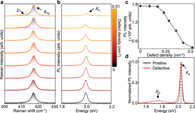
a Evolution of Raman spectra with defect density. A defect-induced (D) mode appears when the defect density is higher than 0.42 nm−2. The spectra are fitted with Lorentzian functions. Signals are presented in arbitrary units (arb. units). b PL spectra evolution with defect density. The neutral A-exciton (XA) PL peak is around 1.98 eV. c Correlation between the A-exciton PL intensity and defect density. Error bars are the standard deviation of three measurements from the same sample. d PL spectra of pristine and defective WS2 at 77 K. The neutral A-exciton (XA) and defect-bound exciton (XD) peaks appear at 2.02 eV and 1.75 eV, respectively. These PL peaks correspond to the electron energy dissipation channels of radiative recombination and electron captured by friction defects, respectively. Source data of (a–d) is provided as a Source Data file.
For further investigation of the electronic properties of defective samples, photoluminescence (PL) spectra evolution for regions with varying defect densities is shown in Fig. 3b. In all spectra, the neutral A-exciton PL peak appears at 1.98 eV, corresponding to the direct band gap at the K point of the Brillouin zone for monolayer WS2. It represents the electron energy dissipation channel of radiative recombination. Analysis of the PL spectra presented in Fig. 3c reveals that when the defect density is below 0.17 nm−2, the neutral A-exciton intensities remain virtually unchanged. As the defect density increases, a gradual reduction in the intensity of the A-exciton peak is observed. Compared to Raman spectroscopy, PL spectroscopy can detect atomic defects with lower densities. Notably, the intensity of the A-exciton for the sample with a defect concentration of 0.51 nm−2 decreased by a factor of three compared to the pristine sample. It suggests that fewer electrons at the conduction band dissipate energy through radiative recombination, which is related to more electrons captured by defects.
To acquire the direct evidence of electrons captured by defects, a low-temperature PL measurement is conducted at 77 K. As illustrated in Fig. 3d, the neutral A-exciton peak appears at 2.02 eV in both pristine and defective regions. In the defective region, an additional defect-induced emission peak at 1.75 eV is observed38. The new peak originates from defect energy levels introduced by friction defects49,50, which are capable of capturing electrons. The electrons in these defect energy levels subsequently undergo radiative recombination with holes in the valence band, forming defect-bound excitons (schematic in Supplementary Fig. 6). This process leads to a reduction of electrons participating in the radiative recombination of neutral A-excitons, which is manifested as a decrease in the A-exciton intensity. The PL results demonstrate that, in addition to the electron energy dissipation channel of radiative recombination, the defective WS2 monolayer provides a new electron energy dissipation channel via electrons captured by friction defects.
Ultrafast dynamic of electronic friction energy dissipation
To elucidate the electron dynamics influenced by friction defects, femtosecond transient absorption spectroscopy (shown in the Methods section and Supplementary Fig. 7) is employed to investigate electron energy dissipation. Through the ultrafast spectroscopy technique, we can obtain insights into the electron energy dissipation channels and rates within defective samples. A pump beam of 2.82 eV (440 nm) is utilized to excite electrons in WS2 with a fluence of 2 µJ cm−2, thereby avoiding nonlinear optical phenomena51,52. It is further confirmed by experiments conducted at varying pump fluences, as shown in Supplementary Fig. 8. The thermal effect is negligible in this study, as the relaxation dynamics are independent of pump fluence. A probe energy is selected as 1.98 eV (625 nm), resonating with the neutral A-exciton of WS2, to monitor the electron dynamics at the conduction band. The change in probe beam reflection ΔR (x, y, t) induced by the pump beam is proportional to the electron density n (x, y, t) at the conduction band minimum of WS2.
The electron energy dissipation dynamics can be obtained from transient absorption signal decay traces with different defect densities, as presented in Fig. 4a. It is evident that with the increase in defect density, the electron energy dissipation rate accelerates, indicating that friction defects enhance the electron energy dissipation. For the pristine sample, the decay trace can be well-fitted by a single exponential function, with a lifetime of about 85 ps. Following the generation of friction defects, the electron dynamics is faster than the pristine sample, and a rapid decay component emerges within the first 10 ps. Thus, to obtain the energy dissipation rates of two energy dissipation channels, we employed a biexponential function convolved with the experimental response function for curve fitting. The slow decay component varies little at around 85 ps with increasing defect density, which is attributed to the radiative recombination of neutral A-exciton53,54. Additionally, the fast decay component occurring at 1 to 10 ps (Supplementary Fig. 9) is ascribed to electrons captured by friction defects50,55,56. The result demonstrates there are two friction energy dissipation channels in defective regions.
Fig. 4: Defect-mediated ultrafast dynamics of electronic friction energy dissipation.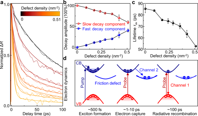
a Transient absorption decay traces with different defect densities of monolayer WS2. The pump and probe wavelengths are 440 nm and 625 nm, respectively. The smooth lines are the fitting curves with biexponential decays convoluted with an experimental response function. b Lifetime amplitude of fast decay (electrons captured by defects) and slow decay (radiative recombination) components as a function of defect density. c The lifetime of a defective WS2 monolayer with different defect densities. Error bars in b and c are the standard deviation of three measurements from the same sample. d Schematic of ultrafast electron dynamics in defective WS2 monolayer. CB: conduction band; VB: valence band. Source data of (a–c) is provided as a Source Data file.
To further clarify the dynamic mechanism of electronic friction energy dissipation induced by defects, it is essential to obtain the energy dissipation rate of defective WS2. We first need to calculate the average energy dissipation lifetime using the formulas, \({\tau }_{{{{\rm{av}}}}}={A}_{1}{\tau }_{1}+{A}_{2}{\tau }_{2}\), where \({\tau }_{1}\) and \({\tau }_{2}\) are the decay lifetime of radiative recombination and electrons captured by friction defects, respectively; \({A}_{1}\) and \({A}_{2}\) are the corresponding normalized amplitude. Analyzing the fitting curves of the decay traces, the evolution of dissipative component amplitude with defect density is revealed in Fig. 4b. As the defect density increases, the amplitude \({A}_{1}\) of radiative recombination decreases from 100% to 59.8%, while the amplitude \({A}_{2}\) of electrons captured by defects increases. The trend is consistent with the significant reduction observed in the neutral A-exciton intensity of our PL spectra. Therefore, the calculated average lifetime \({\tau }_{{{{\rm{av}}}}}\) in Fig. 4c shortens from 85 ps for the pristine sample to 53 ps for the defective sample. Correspondingly, the overall electron energy dissipation rate \({\tau }^{-1}\) increases markedly, which is the reciprocal of the average lifetime \({\tau }_{{{{\rm{av}}}}}\). It suggests that the friction defects in monolayer WS2 lead to an increase in the electron energy dissipation.
The schematic of ultrafast electron dynamics in defective WS2 monolayer is depicted in Fig. 4d. Electrons are pumped to the conduction band within hundreds of femtoseconds, and their energy dissipation channels and rates are subsequently probed using a 1.98 eV probe beam. A portion of the electrons is captured by friction defects within 10 ps, forming a fast energy dissipation channel (Channel 2). Another portion of electrons dissipates energy through radiative recombination at about 100 ps, constituting a slow energy dissipation channel (Channel 1). In other words, in the pristine WS2 sample, the excited electrons primarily dissipate energy through radiative recombination. In contrast, in the defective sample, friction defects introduce defect energy levels within the band structure, which capture electrons in picoseconds. Consequently, the introduction of friction defects provides a new channel for electron energy dissipation, accelerating the electron energy dissipation rate and resulting in increased friction.