
Diffractive waveguide design—multi-mode and single-mode designs
As a proof-of-concept demonstration, we designed a diffractive waveguide to match the performance of a square dielectric waveguide. Figure 1a illustrates the cross-section of a traditional square dielectric waveguide, consisting of core and cladding regions designed to support the propagation of certain spatial modes. The cross-sectional profile of the refractive index of this square dielectric waveguide is shown in Fig. 1b, where the refractive indices of the core and the cladding were selected as \({n}_{{core}}=1.6\) and \({n}_{{cladding}}=1.4\), respectively. Based on this configuration, the spatial modes \(\{{M}_{0},{M}_{1},\ldots\}\) supported by this square dielectric waveguide were calculated using an integrated full-vectorial finite-difference method-based mode solver46,47. In our analysis, the dielectric waveguide used for comparison was assumed to have an ideal refractive index profile, without any material defects and structural inhomogeneities. This assumption effectively eliminates various sources of losses for the standard dielectric waveguides considered in our comparison. Under these conditions, coupling and energy efficiencies are set to 100% for the traditional dielectric waveguides, serving as a reference baseline for evaluating the performance of our diffractive waveguide designs. Our diffractive waveguide, shown in Fig. 1c, was designed to support the propagation of the same target spatial modes and emulate the functionality of the traditional square dielectric waveguide under an illumination wavelength of λ = 0.75 mm. The cascadable unit architecture of our diffractive waveguide design consisted of two layers, spanning a total axial length of 53.3λ, with each layer containing 200 × 200 trainable phase-only diffractive features, each with a size of ~0.53λ. During the training stage of our cascadable diffractive waveguide unit, the first 20 spatial modes \(\{{M}_{0},{M}_{1},\ldots {M}_{19}\}\), calculated based on the assumed square dielectric waveguide cross-section (Fig. 1b), were fed as the complex-valued inputs to the diffractive waveguide input aperture. The phase modulation values of the diffractive features at each layer were iteratively optimized using stochastic gradient descent (SGD) to minimize a training loss function, which ensured the preservation of the targeted modes both in structural consistency (phase and amplitude) and output energy efficiency (see the “Methods” section). After its training, the resulting diffractive waveguide unit (Fig. 1d) could match the mode guiding performance of a traditional square dielectric waveguide (Fig. 1b). Figure 1e visualizes the output fields from both the traditional square dielectric waveguide and the corresponding diffractive waveguide unit, respectively. The optimized diffractive layers exhibit phase modulation patterns, structured at the diffraction limit of light, that sequentially relay the input light as it passes through the successive layers. The corresponding cross-sectional light field profile is also shown in Supplementary Fig. S1. The relative errors between the outputs of the two waveguides (dielectric vs. diffractive) are also displayed, showing that the diffractive waveguide can successfully transmit and maintain the complex-valued spatial modes supported in the traditional square dielectric waveguide with negligible error.
Fig. 1: Comparison between a traditional dielectric waveguide and a diffractive waveguide.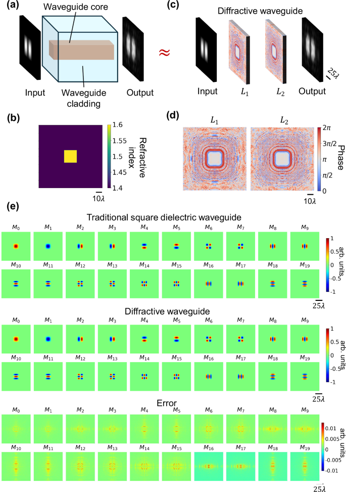
a The cross-section of a traditional square dielectric waveguide consisting of core and cladding dielectric regions, which transmit certain guided spatial modes with high fidelity. b The refractive index cross-sectional profile of the square dielectric waveguide. c Schematic of a cascadable diffractive waveguide unit designed to match the performance of the square dielectric waveguide. d Phase modulation patterns of the trained diffractive layers of the diffractive waveguide. e Output fields from the square dielectric waveguide and the diffractive waveguide are compared, with the relative errors displayed. The output fields of the traditional dielectric waveguide were calculated by a full-vectorial finite-difference method, serving as the ground truth for evaluating the output fields of the diffractive waveguide. The modes are denoted as \({M}_{0} \sim {M}_{19}\).
Besides testing the trained diffractive waveguide with the first 20 spatial modes \(\{{M}_{0},{M}_{1},\ldots,{M}_{19}\}\) used during the training stage, we further evaluated the external generalization ability of the diffractive waveguide using higher-order modes \(\{{M}_{20},{M}_{21},\ldots,\,{M}_{39}\}\) that were never used during training. The results of this comparative analysis for internal and external generalization ability of the diffractive waveguide are illustrated in Fig. 2a, showing a good match between the input and output mode profiles even for higher-order modes \(\{{M}_{20},{M}_{21},\ldots,\,{M}_{39}\}\) never used in training. We also quantified the mode transmission quality of our diffractive waveguide using the coupling efficiency and energy efficiency metrics (see the “Methods” section). As shown in Fig. 2b, the coupling efficiency and the energy efficiency for internal generalization (green region) were consistently higher than 92.0% and 99.4%, respectively. For the higher-order spatial modes (pink region), the coupling efficiency and the energy efficiency remained above 84.0% and 99.0%, respectively. These results indicate that our diffractive waveguide not only learned to support the trained modes of interest (\(\{{M}_{0},{M}_{1},\ldots,{M}_{19}\}\)) but also generalized very well to guide the higher-order modes supported by the refractive index profile of a square dielectric waveguide—although they were never used in the training stage of the diffractive waveguide. To further investigate the coupling efficiency drop observed for higher-order modes, we analyzed the performance of diffractive waveguides trained on different spatial mode sets (see Supplementary Fig. S2). These results show that the coupling efficiency values are significantly improved when all the desired spatial modes of interest are known and accessible during training. Additionally, to account for material absorption in practical implementations, we incorporated energy absorption into the training process, as shown in Supplementary Fig. S3. Compared to designs trained without considering material absorption, those optimized with absorption exhibited improved efficiency when tested with absorbing diffractive materials, demonstrating the benefit of accounting for such factors in the training loss function and optimization process.
Fig. 2: Comparative analysis for internal and external generalization ability of the diffractive waveguide.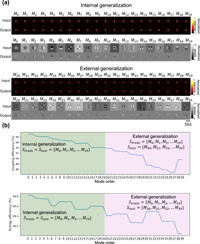
a Intensity and phase profiles of the input and output fields of the diffractive waveguide. Performance was evaluated using two sets of spatial modes: the internal generalization set \(\{{M}_{0},{M}_{1},\ldots,{M}_{19}\}\), which was used during the training stage, and the external generalization set \(\{{M}_{20},{M}_{21},\ldots,{M}_{39}\}\), which was never used during the training. b Coupling efficiency and energy efficiency of the transmitted spatial modes \(\{{M}_{0},\,{M}_{1},\ldots {M}_{39}\}\). The internal generalization performance appears in the green region, and the external generalization performance appears in the pink region.
Next we analyzed the cascading behavior of the optimized diffractive waveguide unit reported in Fig. 2. For this analysis, we cascaded N = 10 identical diffractive waveguide units to achieve a longer propagation distance, as depicted in Fig. 3a. In this cascaded design, any two successive diffractive waveguide units shared a common intermediate plane, i.e., the output field \({o}_{i}\) of the diffractive unit \(i\) served as the input field for the subsequent diffractive unit i + 1. The intensity and phase of the optical field at the input plane, intermediate plane, and output plane are visualized in Fig. 3b, where the intensity patterns were normalized and the phase patterns were adjusted by subtracting a uniform constant phase shift. It can be seen that the spatial modes of the cascaded diffractive waveguide were maintained very well after wave propagation through 10 cascaded diffractive units. Furthermore, the coupling efficiency and the energy efficiency of different modes at each intermediate plane are reported in Fig. 3c, d. These results revealed that: (i) with more diffractive units cascaded, the coupling efficiency of each mode relatively decreased but remained above 91% for all the modes; (ii) the energy efficiency of each mode dropped monotonically with the increase of cascaded diffractive waveguide units but remained over 70% after 10 units; and (iii) higher-order modes experienced a more significant drop in the coupling efficiency and the energy efficiency, which may be due to the higher frequency components contained in these modes, requiring more trainable degrees of freedom in the design of the diffractive waveguide. These results suggest that our diffractive waveguide not only supports the desired modes of interest but also functions as a modular, Lego-like component to be cascaded without further training. This plug-and-play-ready modularity is important for designing solutions to satisfy the needs of various waveguide applications. If needed, however, the overall performance of a cascaded diffractive waveguide of any arbitrary length (N >> 1) can be further improved by using transfer learning and training the cascaded diffractive structure in an end-to-end manner for a given axial length of interest; this would further improve the performance of the diffractive waveguide for a given/desired topology. As reported in Supplementary Fig. S4, when a specific topology is required, end-to-end optimization delivers superior performance in both the coupling efficiency and the energy efficiency compared to the unit-level optimization. While the end-to-end design approach excels in these performance metrics, unit-level optimization is better suited for more general scenarios regardless of the number of cascading units. Moreover, unit-level optimization requires only a one-shot training procedure, unlike the end-to-end approach, which needs to be designed on a case-by-case basis, different for each application.
Fig. 3: Testing results of a cascaded diffractive waveguide for mode transmission.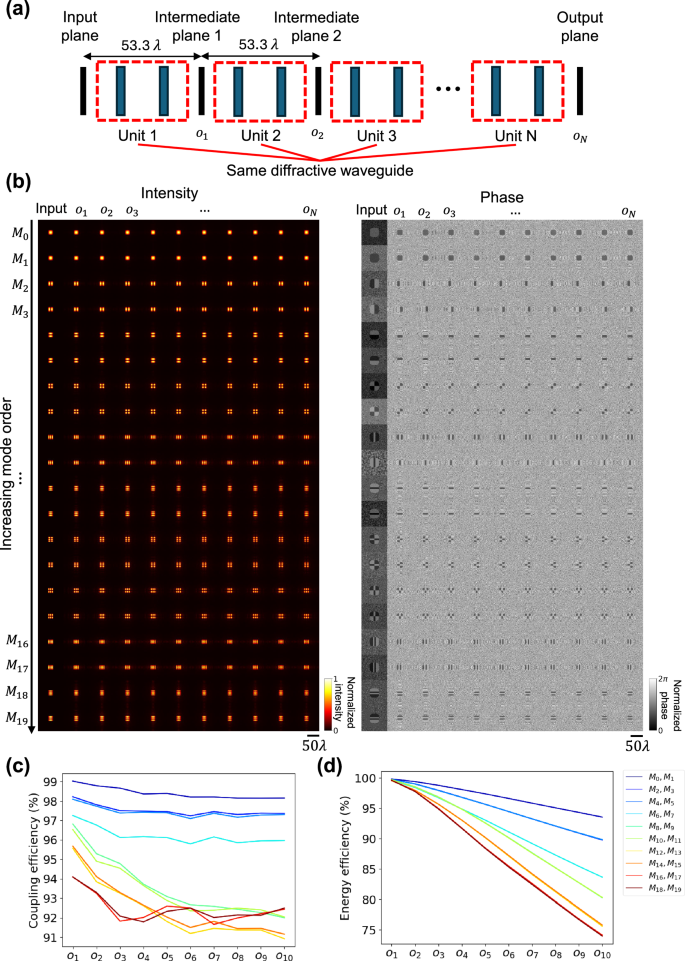
a Schematic of a cascaded diffractive waveguide with \(N\) identical diffractive units. b Intensity and phase profiles of optical fields at the input, intermediate, and output planes. c Coupling efficiency and d energy efficiency of different transmitted modes \(\{{M}_{0},{M}_{1},\ldots,{M}_{19}\}\) at intermediate planes and the output plane. The curves in different colors correspond to different mode orders shown in the legend.
In addition to the multi-mode waveguide designs reported earlier, we also demonstrated single-mode diffractive waveguides. To match the mode profile of a commonly used optical fiber (SMF-28)48 in telecommunication systems, we designed a diffractive waveguide that operates at 1550 nm; see Supplementary Fig. S5. In this infrared waveguide design reported in Supplementary Fig. S5, the feature size of the diffractive layers was scaled down for operation at 800 nm, while the axial distance between successive diffractive layers was selected as 100 μm, corresponding to the common thickness of various glass substrates that can potentially be stacked together. The single-mode transmission behavior and the cascading capability of this diffractive waveguide design were successfully demonstrated and quantified in Supplementary Fig. S5. To explore the feasibility of implementations in the near-infrared part of the spectrum, we conducted simulations at 1550 nm wavelength for approximating the waveguiding behavior of SMF-28 fiber48, which is a single-mode optical fiber that is widely used in telecommunications. As shown in Supplementary Fig. S6, >95% coupling efficiency and >95% energy efficiency can be achieved with 4-bit depth diffractive layers (K = 2), with each layer having a lateral resolution of 1.55 μm. These fabrication specifications in terms of phase bit depth and lateral resolution are compatible with commercial two-photon polymerization-based 3D nanoprinters or lithography-based nanofabrication technologies. Especially wafer-scale high-throughput fabrication of such diffractive designs using high-purity fused silica that has an ultra-low loss and high thermal stability, as demonstrated in recent work49, holds promise for mass-scale fabrication of cascadable diffractive waveguides operating in the near-infrared spectrum42,50. As another example of a single-mode diffractive waveguide design with a tighter mode diameter, we selected 532 nm as our operation wavelength, where the resulting diffractive design confined the full width at half maximum of the spatial mode supported by the diffractive waveguide to \(\sim 6.4\lambda\) = 3.4 µm, as shown in Supplementary Fig. S7. These results illustrate the diffractive waveguide’s capability to confine single-mode light within a tight modal profile, comparable to traditional planar, strip-on-chip waveguides, underscoring its potential for broader applications.
Although the diffractive waveguides demonstrated so far exhibit increased total energy loss with longer propagation distances, it is crucial to highlight that their versatile functionalities—such as mode filtering and mode splitting— provide some unique features. Unlike optical fibers, which are optimized for long-distance transmission, one of the key objectives of these diffractive waveguides is to provide greater design flexibility for short-range transmission and light processing applications, such as, e.g., on-chip optical interconnects, multiplexed routing, and distributed sensors. Diffractive waveguides and the design framework behind them expand the range of tools available for creating customized waveguide designs tailored for various spatial, spectral, and/or polarization-based light processing, multiplexing, and routing needs.
Bent diffractive waveguide design
One of the important functions of waveguides is to efficiently guide and redirect light. To address this need, we designed a bent diffractive waveguide to redirect the guided modes of light and provide an interface that can be directly cascaded with the linear diffractive waveguide design described in the previous sub-sections. Figure 4a illustrates the structure of a bent diffractive waveguide with four layers, in which the light propagation direction was rotated by \({45}^{\circ }\) from the input to the output plane. Here, the input plane is parallel to the first diffractive layer, and the output plane is parallel to the last diffractive layer. Starting from the second diffractive layer of the bent waveguide design, a \({15}^{\circ }\) clockwise rotation was performed relative to the normal direction of the previous plane, culminating in \({45}^{\circ }\) rotation in total. The tilted angular spectrum method51 was used to simulate light propagation between the adjacent diffractive layers, and these diffractive layers were trained to minimize the structural difference between the input optical modes and the output optical fields based on the coupling efficiency metric, while also maximizing the output energy efficiency (see the “Methods” section for details). Once the training converged, the trained diffractive layers, as shown in Fig. 4b, were numerically tested with the optical modes of the same dielectric square waveguide, including both \(\{{M}_{0} \sim {M}_{19}\}\) that were used in training (internal generalization) and the higher-order modes \(\{{M}_{20} \sim {M}_{39}\}\) that were never used in training (external generalization). The intensity and phase profiles of the input and the transmitted optical fields at the output are visualized in Fig. 4c, showing that all the modes \(\{{M}_{0} \sim {M}_{39}\}\) could be maintained after propagating through the bent diffractive waveguide. Figure 4d reports the coupling efficiency and the energy efficiency of these spatial modes after transmitting through the bent diffractive waveguide. The coupling efficiency for internal generalization remained >90% while the energy efficiency was greater than 60%. Although the higher-order modes \(\{{M}_{20} \sim {M}_{39}\}\) were never used during the training process, the bent diffractive waveguide achieved >75% coupling efficiency and >65% energy efficiency for these modes, indicating the success of the bent diffractive waveguide design.
Fig. 4: The structure and testing results of a bent diffractive waveguide.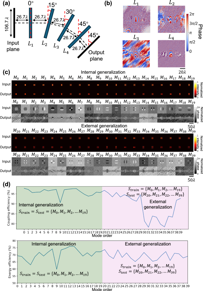
a Illustration of a bent diffractive waveguide. b Phase modulation patterns of the converged diffractive layers of the bent diffractive waveguide. c Intensity and phase profiles of the input and output fields of the bent diffractive waveguide. Performance was evaluated using two sets of spatial modes: an internal set \(\{{M}_{0},{M}_{1},\ldots,{M}_{19}\}\), which was used during the training, and an external set \(\{{M}_{20},{M}_{21},\ldots,{M}_{39}\}\), which was never used during the training. Each row of output images is separately normalized. d Coupling efficiency and energy efficiency of the transmitted modes \(\{{M}_{0},{M}_{1},\ldots,{M}_{39}\}\) at the output plane. The internal generalization performance appears in the green region, and the external generalization performance appears in the pink region.
To further investigate the impact of the number of diffractive layers and the rotation angle between two successive layers on the performance of the tilted diffractive waveguide, various designs with different numbers of layers and bending angles were explored. As shown in Supplementary Fig. S8, increasing the number of diffractive layers for a fixed total bending angle improved waveguide performance due to the greater design flexibility and larger degrees of freedom available, leading to better coupling efficiencies. Additionally, the influence of different total bending angles while maintaining a constant turn step (11.25°) and a constant axial distance between two successive layers (26.67λ) was also examined; see Supplementary Fig. S9. While the coupling efficiency remained consistent among different conditions, the energy efficiency slightly declined with increasing propagation distance and bending angle. Notably, there is no single optimal solution as each diffractive waveguide design can be optimized based on specific application requirements. These analyses underscore the flexibility of diffractive waveguide designs, enabling tailored solutions for various desired performance specifications.
Mode filtering diffractive waveguide design
Spatial mode filters are foundational in controlling the transmission and rejection of specific guided modes, essential for various optical and photonic applications, including, e.g., optical communications, microscopy, and laser engineering20,21,22. However, these filters are often bulky, costly, and difficult to integrate into compact systems52,53. Additionally, traditional waveguide filters struggle to precisely control the spatial mode selections based on the mode number and/or frequency. Our diffractive waveguides can be designed by appropriately tailoring the training loss function for a specific desired task, providing a versatile approach to cover various applications. To showcase this, we designed mode filtering diffractive waveguides capable of selectively passing or rejecting certain spatial modes of interest. These mode filtering diffractive waveguides were precisely optimized to transmit desired modes while effectively blocking unwanted guided modes. We demonstrated this capability through two different designs: a high-pass mode filtering waveguide and a bandpass mode filtering waveguide. The high-pass filtering waveguide differentiated between a target set of modes to be passed/transmitted, i.e., \({S}_{t}=\{{M}_{12},\,{M}_{13},{M}_{14},\ldots {M}_{19}\}\) and a rejection mode set, i.e., \({S}_{r}=\{{M}_{0},{M}_{1},{M}_{2},\ldots,{M}_{11}\}\); in this first design, we preserved the energy efficiency and mode patterns for the target set \({S}_{t}\) while filtering out the guided modes of the rejection set Sr—see Supplementary Fig. S10a. In the second mode filtering diffractive waveguide design, we aimed at bandpass filtering, where the transmission set was defined as \({S}_{t}=\left\{{M}_{0},{M}_{1}\right\}\cup \left\{{M}_{6} \sim {M}_{11}\right\}\cup \{{M}_{16} \sim {M}_{19}\}\) and the rejection set was defined as \({S}_{r}=\left\{{M}_{2} \sim {M}_{5}\right\}\cup \left\{{M}_{12} \sim {M}_{15}\right\}.\)
To design these mode filtering diffractive waveguides, four hyperparameters were defined: \({T}_{{CE},u},{T}_{{CE},l},{T}_{E,u}\) and \({T}_{E,l}\), which set the upper (\(u\)) and lower (\(l\)) thresholds of the coupling efficiency \(({T}_{{CE},u},{T}_{{CE},l})\) and the energy efficiency (\({T}_{E,u}\) and \({T}_{E,l}\)), respectively. By adjusting these threshold values and following a similar training process as described in the previous sub-sections, mode filtering diffractive waveguide designs with different passband and rejection band metrics could be achieved (see the “Methods” section for details). Supplementary Fig. S10b reports the input and output patterns of the high-pass mode filtering diffractive waveguide along with the resulting coupling efficiency and energy efficiency values. This high-pass mode filtering diffractive waveguide design successfully rejected, as expected/desired, unwanted lower-order modes with an energy efficiency \( and a coupling efficiency \(\sim 3\%\), and allowed the desired spatial modes with \( > 50\%\) energy efficiency and \( > 90\%\) coupling efficiency. Similarly, the results of the bandpass mode filtering diffractive waveguide design are shown in Supplementary Fig. S10c, where \({S}_{r}=\left\{{M}_{2} \sim {M}_{5}\right\}\cup \left\{{M}_{12} \sim {M}_{15}\right\}\) were rejected with low coupling efficiency and energy efficiency values, and \({S}_{t}=\left\{{M}_{0},{M}_{1}\right\}\cup \left\{{M}_{6} \sim {M}_{11}\right\}\cup \{{M}_{16} \sim {M}_{19}\}\) were transmitted through the diffractive waveguide with high quality. These results underscore the effectiveness of our mode filtering diffractive waveguide designs. By tuning the thresholds (\({T}_{{CE},u},{T}_{{CE},l},{T}_{E,u}\) and \({T}_{E,l}\)) during the training stage, one can further design diffractive waveguides with different sets of guided modes that are selectively transmitted and rejected, streamlining the design of mode filtering diffractive waveguides for various applications.
To further demonstrate the unique capabilities of these mode filtering diffractive waveguide designs, a multi-wavelength mode filter was developed, as shown in Fig. 5a. This diffractive waveguide was optimized to selectively transmit different sets of spatial modes at certain illumination wavelengths. Specifically, the spatial modes in \({S}_{{\lambda }_{1}}=\{{M}_{0},{M}_{1}\}\), \({S}_{{\lambda }_{2}}\,=\{{M}_{6}\, \sim {M}_{11}\}\) and \({S}_{{\lambda }_{3}}=\left\{{S}_{16} \sim {S}_{19}\right\}\) can only transmit at the corresponding illumination wavelengths λ1 = 0.7 mm, λ2 = 0.75 mm, and λ3 = 0.8 mm, respectively. All other modes were filtered out through this multi-wavelength mode filtering diffractive waveguide. Following a similar training strategy used for its monochromatic counterpart, the multi-wavelength design was effectively optimized to select distinct sets of modes at different illumination wavelengths. Figure 5b illustrates the input and output patterns across different wavelengths. The resulting coupling efficiency and the energy efficiency values, shown in Fig. 5c, further highlight the success of the multi-wavelength filter function, where the desired, transmitted modes maintain high quality, and the rejected modes exhibit low coupling and energy efficiencies within the targeted wavelengths. By adjusting the loss function during the training phase, diffractive waveguides with tailored functionalities for more advanced mode filtering across specific mode orders and wavelengths can be achieved.
Fig. 5: Testing results of a multi-wavelength mode filtering diffractive waveguide.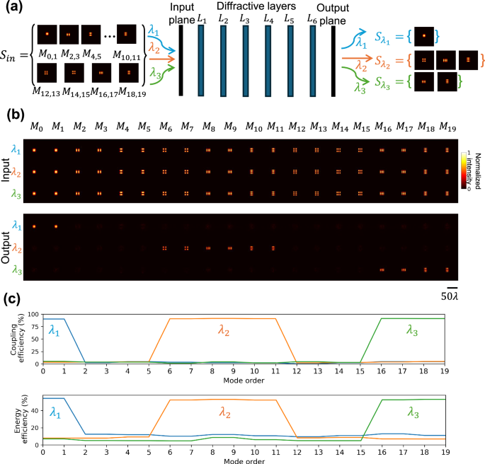
a Schematic of a multi-wavelength mode filtering diffractive waveguide designed to pass different sets of modes at different illumination wavelengths. Spatial modes in \({S}_{{\lambda }_{i}}\) can only be transmitted at the corresponding illumination wavelength \({\lambda }_{i}\) (\(i=1,2,3\)). b Intensity profiles of the input and output fields of the multi-wavelength mode filtering diffractive waveguide. c Coupling efficiency and energy efficiency of all the input spatial modes at different illumination wavelengths.
Mode splitting diffractive waveguide design
Different from the monochromatic and multicolor mode filtering diffractive waveguide designs reported in earlier sub-sections, here we consider the design of a diffractive waveguide that performs mode splitting from the input field of view (FOV) to separate regions in the output FOV (detailed in the “Methods” section). As illustrated in Supplementary Fig. 11a, the input modes \({S}_{{in}}=\{{M}_{0},{M}_{1},\ldots,\,{M}_{19}\}\) entering the input FOV were separated into two output channels based on their spatial mode order: lower-order modes in \({S}_{{CH}1}=\{{M}_{0},{M}_{1},\ldots,{M}_{11}\}\) were directed to Channel 1, while the higher-order modes in \({S}_{{CH}2}=\{{M}_{12},{M}_{13},\ldots,{M}_{19}\}\) were directed to Channel 2. To optimize this mode splitting diffractive waveguide, we superimposed spatial modes of varying orders and minimized the mean square error (MSE) between the presumed weights for the input mode combination and the decomposed weights derived from the target spatial mode at each output channel. The resulting trained diffractive layers are reported in Supplementary Fig. 11b. To blindly test this mode splitting diffractive waveguide design, we sequentially input different modes at the input FOV; see Supplementary Fig. 11c. The mode splitting diffractive waveguide successfully guided all the modes in \({S}_{{CH}1}=\{{M}_{0},{M}_{1},\ldots,{M}_{11}\}\) into Channel 1, while the modes in the second set \({S}_{{CH}2}=\{{M}_{12},{M}_{13},\ldots,{M}_{19}\}\) were directed to Channel 2—as targeted/desired. Furthermore, the coupling efficiency and the energy efficiency of the two channels for all the spatial modes of interest were quantified in Supplementary Fig. 11d, showing a good mode splitting performance, also suppressing the energy of the unwanted modes in each output channel. We also trained mode splitting diffractive waveguides with different numbers (K) of diffractive layers in each unit, revealing that the energy efficiency for both output channels increased with more diffractive layers, showcasing the advantages of deeper diffractive designs with more degrees of freedom (see Supplementary Fig. 11d). Although the coupling efficiency of the filtered modes in CH1 was appreciable, the corresponding energy efficiency was notably diminished—as desired, indicating that only a minimal amount of energy was coupled into these specific spatial modes. In various applications such as wavelength-division multiplexing (WDM) and mode-division multiplexing (MDM), the energy efficiency serves as a more critical parameter for evaluating performance. We also observed that the coupling efficiency of suppressed modes in CH1 and CH2 differed, which can be attributed to the hyperparameters \(\alpha\) and \(\beta\), which were adjusted to balance the coupling efficiency and energy efficiency. In this work, the energy efficiency was prioritized, as it is essential for the optimal performance of the mode filtering diffractive waveguide. To assess the influence of these hyperparameters, \(\alpha\) in Eq. 19 was varied from 10 to 50 in increments of 10. The results, presented in Supplementary Fig. S12, revealed that increasing \(\alpha\) led to a further reduction in the coupling efficiency of the filtered modes—as desired.
In a more general scenario, spatial modes with multiple wavelengths within a single input aperture can also be demultiplexed into different channels. To demonstrate this capability, we report a multi-wavelength mode splitting diffractive waveguide that can split the input aperture into 2 × 2 outputs based on the order of the spatial modes and illumination wavelengths. As illustrated in Fig. 6a, the input modes in two different illumination wavelengths entering the input aperture were separated into four output channels based on their wavelength and spatial mode order: at illumination wavelength λ1 = 0.7 mm, modes in \({S}_{{CH}1}=\{{M}_{0} \sim {M}_{11}\}\) and \({S}_{{CH}2}=\left\{{M}_{12} \sim {M}_{19}\right\}\) were directed into Channel 1 and Channel 2, respectively; at illumination wavelength λ2 = 0.8 mm, modes in \({S}_{{CH}3}=\{{M}_{0} \sim {M}_{7}\}\) and \({S}_{{CH}4}=\left\{{M}_{8} \sim {M}_{19}\right\}\) were directed into Channel 3 and Channel 4, respectively. The trained model was blindly tested with different orders of optical modes at these two illumination wavelengths individually, shown in Fig. 6b. At \({\lambda }_{1}\) illumination, the multi-wavelength mode splitting diffractive waveguide successfully guided all the modes in \({S}_{{CH}1}\) into Channel 1 and the other modes in \({S}_{{CH}2}\) into Channel 2 while exhibiting no apparent crosstalk with Channels 3 and 4. Similarly, Channels 3 and 4 were able to receive their desired set of modes at the illumination wavelength \({\lambda }_{2}\) with no evident leakage into Channels 1 and 2. Furthermore, we quantified the coupling efficiency and the energy efficiency of these four output channels for all spatial modes of interest in Fig. 6c, showing a good mode splitting performance and suppression of unwanted modes in each output channel.
Fig. 6: Testing results of a multi-wavelength mode splitting diffractive waveguide.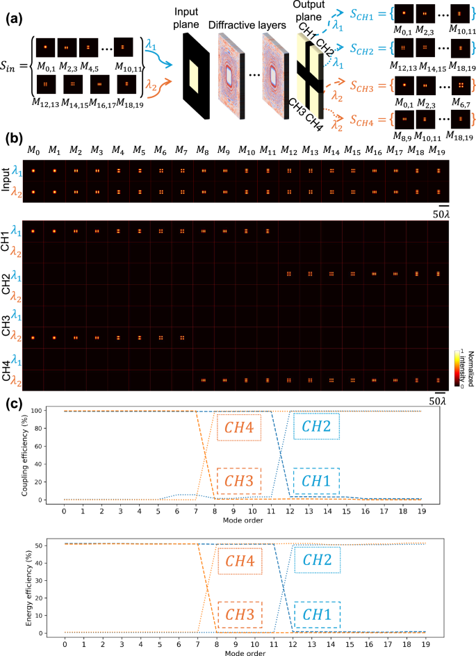
a Schematic of a multi-wavelength mode splitting diffractive waveguide, designed to split modes from the input aperture to separate regions in the output aperture, depending on both the order of the spatial modes and the wavelengths. b Blind testing results: the intensity profiles of the input fields and the output fields at the four output channels of the multi-wavelength mode splitting diffractive waveguide. Each row of output images was separately normalized. c Coupling efficiency and energy efficiency of the four output channels for the transmitted modes \(\{{M}_{0},{M}_{1},\ldots,{M}_{19}\}\) at the output plane.
Mode-specific polarization-maintaining diffractive waveguide
We also designed mode-specific polarization-maintaining diffractive waveguides using a combination of optimized diffractive layers and PAs as illustrated in Fig. 7a. The PA consisted of multiple linear polarizer units with four different polarization directions: 0°, 45°, 90°, and 135°, which repeat periodically over space—i.e., non-trainable. The mode-specific polarization-maintaining diffractive waveguide was designed to maintain the \(\hat{x}\) polarization state of the spatial modes in \({S}_{\hat{x}}=\{{M}_{0},{M}_{1},{M}_{4},{M}_{5},{M}_{8},{M}_{9},{M}_{12},{M}_{13},{M}_{16},{M}_{17}\}\) while blocking all the spatial modes in \({S}_{\hat{y}}=\{{M}_{2},{M}_{3},{M}_{6},{M}_{7},{M}_{10},{M}_{11},{M}_{14},{M}_{15},{M}_{18},{M}_{19}\}\). Symmetrically, it maintained the \(\hat{y}\) polarization state of the spatial modes in \({S}_{\hat{y}}\) while blocking all the spatial modes in \({S}_{\hat{x}}\), as depicted in Fig. 7b. Figure 7c shows the coupling efficiency and the energy efficiency for the modes with the correct set of mode order and polarization state, while all the other undesired combinations of modes and polarization states were effectively filtered out. These results indicate that our mode-specific polarization-maintaining diffractive waveguide can be designed to maintain different sets of modes at different polarization states. The cascading behavior of this mode-specific polarization-maintaining diffractive waveguide was also investigated, reported in Supplementary Fig. 13. In this analysis, we cascaded N = 5 identical polarization-maintaining diffractive waveguide units to achieve a longer propagation distance, following a similar approach to the cascading diffractive waveguide design reported in Fig. 3. The intensity of the optical field at the input plane, intermediate planes, and output plane are visualized in Supplementary Fig. 14a. Moreover, the coupling efficiency and the energy efficiency of different guided modes, across all combinations of input and output polarization states at each intermediate plane, are presented in Supplementary Fig. 14b, which further illustrate the plug-and-play-ready feature of each polarization-maintaining diffractive waveguide unit, cascaded to each other, one following another.
Fig. 7: The structure and testing results of a mode-specific polarization-maintaining diffractive waveguide.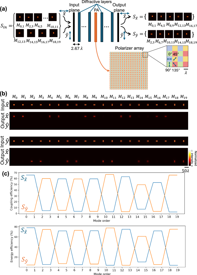
a Illustration of a mode-specific polarization-maintaining diffractive waveguide. Spatial modes in each set can only be transmitted at a specific input polarization direction. The polarization array consists of multiple linear polarizer units with four different polarization directions: 0°, 45°, 90°, and 135°, which repeat periodically. b Blind testing results: the intensity profiles of the input fields and the output fields at two orthogonal linear polarization states (\(\hat{x}\) and \(\hat{y}\)). Output images from the same input polarization direction were normalized together. c Coupling efficiency and energy efficiency of the transmitted modes at different combinations of input and output polarization directions.
Experimental demonstration of mode filtering diffractive waveguides
We experimentally demonstrated the proof of concept of our mode filtering diffractive waveguide design using terahertz radiation. For this, we trained a three-layer mode filtering diffractive waveguide to selectively allow \(\{{M}_{6},\,{M}_{7}\}\) to pass through while rejecting the other spatial modes, as shown in Fig. 8a. Accordingly, we adjusted the hyperparameters \(\left({T}_{{CE},u},{T}_{E,u},{T}_{{CE},l},{T}_{E,l}\right)=({\mathrm{0.85,0.5,0.05,0.05}})\) (detailed in the “Methods” section). Numerical analysis of the coupling efficiency and the energy efficiency of the resulting design confirmed that the mode filtering diffractive waveguide was successfully trained to selectively pass the specific spatial modes \(\{{M}_{6},\,{M}_{7}\}\) as shown in Fig. 9a. After the training stage, the resulting diffractive layers (Fig. 8b) were 3D printed, physically forming a mode filtering diffractive waveguide. This assembled diffractive waveguide was then experimentally tested under a THz scanning system shown in Fig. 8c, d.
Fig. 8: Experimental validation of the mode filtering diffractive waveguide using terahertz radiation.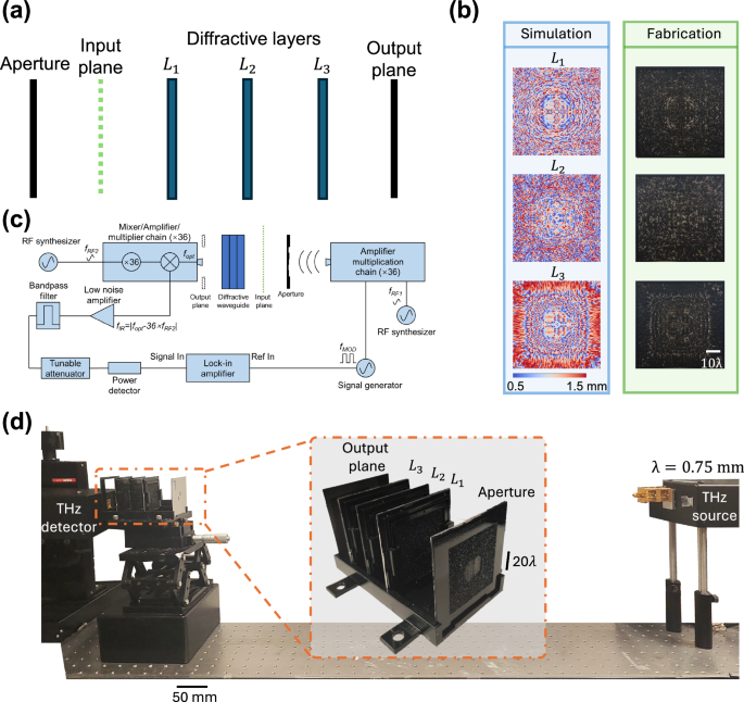
a Design schematic of a three-layer bandpass mode filtering diffractive waveguide, which passed \(\{{M}_{6},\,{M}_{7}\}\) and rejected the other spatial modes. b Left: Height profiles of the trained diffractive layers. Right: The fabricated diffractive layers used in the experiment. c Diagram of the terahertz scanning system. d Photograph of the experimental setup and the 3D-printed diffractive mode filter.
Fig. 9: Testing results of the bandpass mode filtering diffractive waveguide.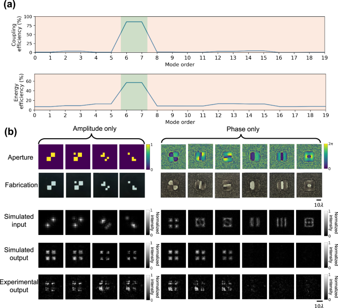
a Numerical analysis of the trained bandpass mode filtering diffractive waveguide in terms of coupling efficiency and energy efficiency. b Experimental results of the bandpass mode filtering diffractive waveguide, designed to pass only\(\,\{{M}_{6},{M}_{7}\}\).
For the experimental testing of our 3D-printed mode filtering diffractive waveguide, we fabricated four amplitude-only apertures and six phase-only apertures, which were used to generate structured optical fields, containing certain spatial modes at the input plane, as illustrated in the first and the second rows of Fig. 9b (see the “Methods” section for details). For these 10 input test apertures, all the amplitude-only apertures and the first three phase-only apertures could excite the input modes \(\{{M}_{6},{M}_{7}\}\); the input fields produced by the remaining three phase-only input apertures did not include these target spatial modes. The output FOV of the mode filtering diffractive waveguide was scanned for each one of these 10 test input apertures using a THz detector, forming the output images displayed in the fourth row of Fig. 9b. These experimental results showed a decent agreement with the numerical simulation results and revealed that the 3D fabricated mode filtering diffractive waveguide effectively filtered out undesired spatial modes while permitting the transmission of the target spatial modes \(\{{M}_{6},{M}_{7}\}\)—as desired in its design. The relatively small mismatch between the numerical simulation and experimental results may originate from the imperfections of the 3D fabrication and the misalignments between the diffractive layers, which can be mitigated by taking these factors into account during the training phase through, e.g., a numerical vaccination process54.
In addition to our monochromatic experimental results, we also designed a multi-wavelength mode filtering diffractive waveguide to pass different sets of modes at different illumination wavelengths, as depicted in Fig. 10a. We followed the same process mentioned in the monochrome design while involving two illumination wavelengths, λ1 = 0.7 mm and λ2 = 0.8 mm. Once the model converged, the diffractive layers were 3D printed and aligned, as shown in Fig. 10b. We numerically calculated the coupling efficiency and the energy efficiency at the output plane for spatial modes at different illumination wavelengths, as shown in Fig. 10c. This multi-wavelength mode filtering diffractive waveguide design successfully passed \(\{{M}_{2},{M}_{3}\}\) at the illumination wavelength λ1 = 0.7 mm and passed \(\{{M}_{12},{M}_{13}\}\) at the illumination wavelength λ2 = 0.8 mm, while rejecting all other modes at both wavelengths. The fabricated multi-wavelength mode filtering diffractive waveguide was tested experimentally using four different phase-only apertures. These 3D-printed phase apertures, as illustrated in the first and second columns of Fig. 10d, were used to generate specific structured optical fields at different illumination wavelengths, shown in the third and fourth columns of Fig. 10d, which contained different ratios of optical modes. The first phase aperture could excite the corresponding target modes for both illumination wavelengths, the second and third apertures could individually excite the target modes at different wavelengths, while the optical field produced by the fourth phase aperture did not include any target modes. The outputs of this 3D fabricated multi-wavelength mode filtering diffractive waveguide were numerically simulated and experimentally measured using the same setup. Cross-correlation operation was used to evaluate the similarity between the experimental results and the simulated/numerical results (see the “Methods” section), which showed a good agreement between the two, experimentally demonstrating the effective mode filtering functionality of the 3D-printed multi-wavelength mode filtering waveguide.
Fig. 10: Experimental validation of the multi-wavelength mode filtering diffractive waveguide.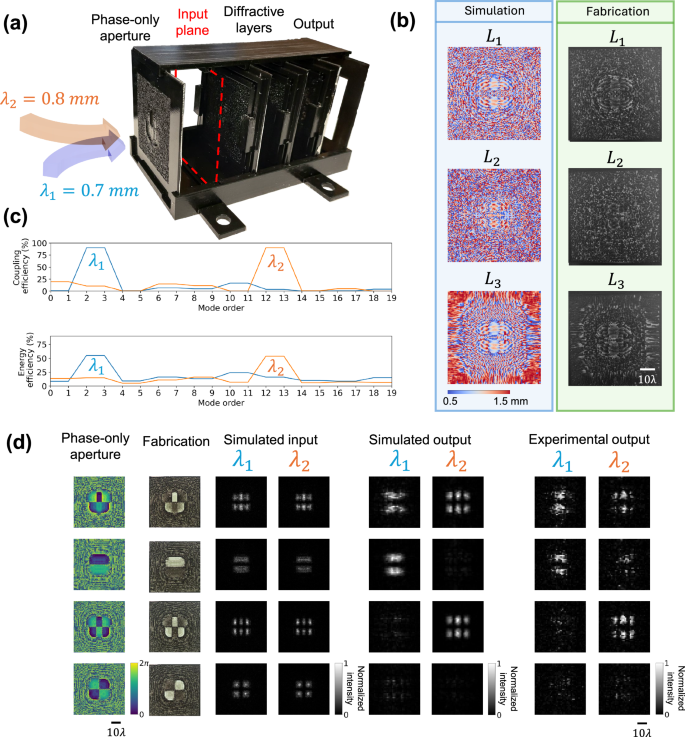
a Photograph of the experimental setup and the 3D-printed multi-wavelength diffractive mode filter. b Left: Height profiles of the trained diffractive layers. Right: The fabricated diffractive layers used in the experiment. c Numerical analysis of the trained multi-wavelength mode filtering diffractive waveguide under different illumination wavelengths in terms of the coupling efficiency and the energy efficiency. d Experimental results of the multi-wavelength mode filtering diffractive waveguide, designed to pass \(\{{M}_{2},{M}_{3}\}\) at λ1 = 0.7 mm and \(\{{M}_{12},{M}_{13}\}\) at λ2 = 0.8 mm.