A novel fabrication approach developed by collaborating scientists at some of the top universities in the UK now allows for the insertion and real-time monitoring of quantum defects in diamonds. This is a crucial step in developing scalable quantum technologies as the world takes the technological leap into a world powered by quantum states and their unique properties.
Knowledge about quantum states has existed for a while, but it is only now that we can leverage this information for practical applications. Quantum computing and sensing can radically change the way the world operates today. Unlocking quantum states opens up possibilities for many applications at scales never imagined before.
For instance, quantum computers can complete operations in minutes, which even the fastest supercomputers would take decades to crunch on. Quantum sensing, on the other hand, can improve the accuracy and sensitivity of various applications by several orders of magnitude. However, for these technologies to become mainstream, they must be scalable.
Scaling up quantum features
Researchers at the universities of Oxford, Cambridge, and Manchester in the UK collaborated on developing Group IV quantum defects in diamonds. These tiny imperfections in diamond crystals help store and transmit quantum information.
These can be used to develop highly scalable quantum networks that deliver highly secure and ultrafast quantum networks. Group IV quantum defects can be generated by introducing elements like silicon, tin, or germanium in diamond. These defects act as spin-photon interfaces, where they connect ‘spin’ information of the electron stored in qubits to photons.
While Group IV centers have been known for their high degree of symmetry with optical and spin properties, reliably achieving them has been a major hurdle until now. A two-step fabrication method developed by researchers in the UK allows this process to be completed in real-time.
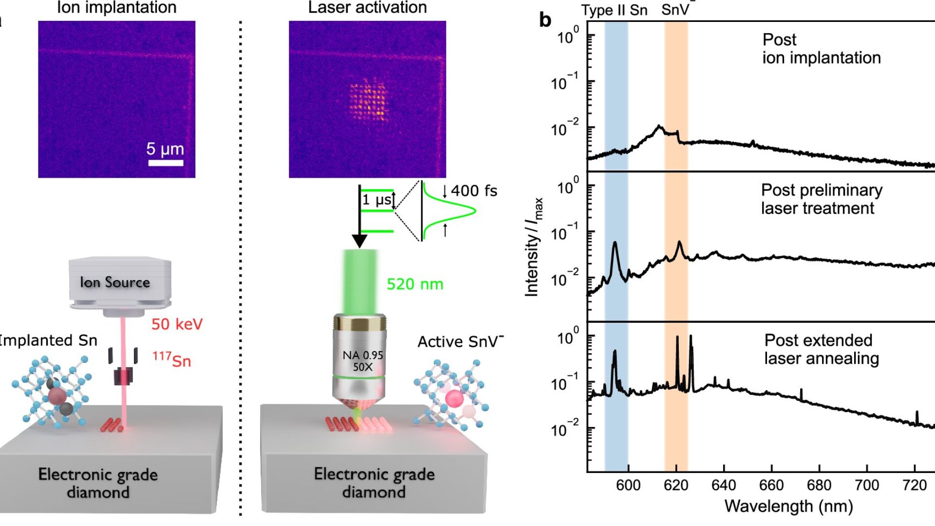 Laser activation of tin-related defect centers. Image credit: Nature Communications.
How did they do it?
The researchers placed single tin atoms into synthetic diamonds and then used an ultrafast laser to activate them. The team deployed a focused ion beam platform, which allowed them to place tin ions individually in exact positions within the diamond but with nanometer accuracy.
Using laser annealing, the researchers implanted the tin atoms into tin-vacancy color centers, which excites the tiny regions of the diamond without damaging them. The approach also results in spectral feedback, facilitating real-time defect monitoring while the process progresses.
Since the scientists can now spot when the defect is activated, they can control the laser activity, giving them immense control over the entire process.
“What is particularly remarkable about this method is that it enables in-situ control and feedback during the defect creation process,” said Andreas Thurn, a postdoctoral researcher at the University of Cambridge, in a press release.
“This means we can activate quantum emitters efficiently and with high spatial precision—an important tool for creating large-scale quantum networks. This approach is not limited to diamond; it is a versatile platform that could be adapted to other wide-bandgap materials.”
The research findings were published in the journal Nature Communications.