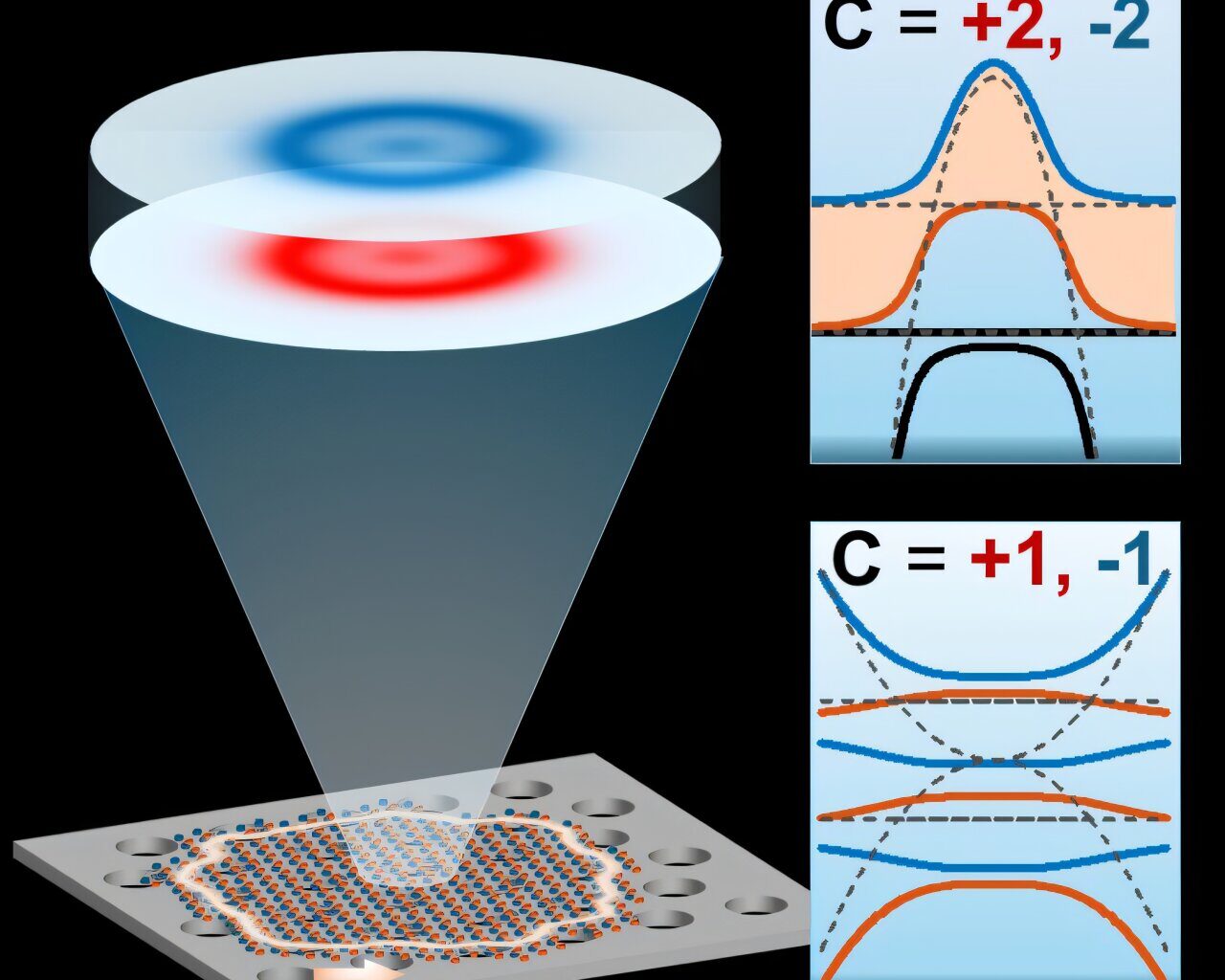
 as it moves through the bulk crystal, giving rise to distinct curvature distributions and opposite nonzero Chern numbers. Credit: Physical Review X (2025). DOI: 10.1103/PhysRevX.15.021061")
Light conducts around the edge of a simulated topological insulator, shown at the bottom of image. The topological insulator is made from a layer of a 2D material resting atop a photonic crystal. The red and blue insets illustrate how the light wave twists differently in two example isolated bands (selected from the band structures shown in the right panels) as it moves through the bulk crystal, giving rise to distinct curvature distributions and opposite nonzero Chern numbers. Credit: Physical Review X (2025). DOI: 10.1103/PhysRevX.15.021061
The candidate pool for engineered materials that can help enable tomorrow’s cutting-edge optical technologies—such as lasers, detectors and imaging devices—is much deeper than previously believed.
That’s according to new research from the University of Michigan that examined a class of materials known as topological insulators. These materials have exciting and tunable properties when it comes to how they transmit energy and information.
“We see this as a step toward building a more versatile and powerful foundation for future photonic technologies,” said Xin Xie, a research fellow in the U-M Department of Physics and lead author of the recent study in the journal Physical Review X.
Although these futuristic materials may sound intimidating, their fundamentals are pretty straightforward. Here, the word insulator has the same meaning as it does in elementary electronics: It’s a material that blocks the flow of something, for example, wood or rubber in the case of electricity.
A topological insulator is an insulator with a twist. It’s mostly an insulator, but it has a special feature where its outer surface, whatever shape it may be, is conductive. This opens up new possibilities for researchers to control the flow of electricity or light and put those to work in new applications.
The U-M team was interested in a particular type of topological insulator that confines conduction to its edge while allowing a single direction of flow. There are comparable materials being developed in electronics and researchers have been interested in expanding that performance to light, said Hui Deng, senior author of the study and U-M professor of physics.
“There’s a lot of interest in these systems for transporting photonic information,” she said. “They have unidirectional transport and the light can go around defects without scattering.”
It’d be natural to assume, given the systems’ strict performance criteria, the list of ways to make them would be rather exclusive. In fact, at present, researchers have focused on just a single way to unlock those properties with help from an external magnetic field.
This largely has to do with a physical property of the system called its band gap. This can be thought of as an energetic hurdle inside the system that needs to be cleared for light or electrons to access a conducting state.
The topological insulator’s band gap gives rise to its unique conductive properties. The size of a band gap is also important. Larger band gaps help “protect” the special edge conduction state, Deng said.
Following design principles from their electronic counterparts, researchers working on these photonic topological insulators had largely focused on a single type of band gap. But the U-M team, which also included Kai Sun, professor of physics, used symmetry analysis and computer simulations to probe other approaches.
In electronics, the band structure is controlled by the crystal structure of the material’s atoms. For optical devices, researchers create “photonic crystals” by fabricating arrays of pits, pillars or other periodic nanoscale features that give rise to a system’s optical properties, including its band structure and band gap.
Discover the latest in science, tech, and space with over 100,000 subscribers who rely on Phys.org for daily insights.
Sign up for our free newsletter and get updates on breakthroughs,
innovations, and research that matter—daily or weekly.
Coupling certain photonic crystal designs with atomically flat 2D materials created the topological insulators the team was after, according to its simulations. But the simulated systems had band structures that were different from that single type previously being focused on.
That means the design portfolio for this class of topological insulators—called polariton Chern insulators—is unexpectedly broad, the researchers said. For instance, the team took as a case study a type of photonic crystal that’s already used in other areas of optical research.
“What surprised me most was how common the required band structures actually are,” Xie said. “Even standard photonic crystal designs—long used in other contexts—can readily support polariton Chern insulators, delivering remarkable performance enhancements.”
The next step for the team is fabricating real examples of the systems they’ve simulated, which is no trivial feat, but such experiments are a strength of Deng’s team. When such a topological insulator is built in a lab, the researchers’ work estimates its band gap could be up to about 100 times larger than the current record.
More information:
Xin Xie et al, Polariton Chern Bands in 2D Photonic Crystals beyond Dirac Cones, Physical Review X (2025). DOI: 10.1103/PhysRevX.15.021061
Provided by
University of Michigan
Citation:
More pathways than previously thought can lead to optical topological insulators (2025, June 24)
retrieved 25 June 2025
from https://phys.org/news/2025-06-pathways-previously-thought-optical-topological.html
This document is subject to copyright. Apart from any fair dealing for the purpose of private study or research, no
part may be reproduced without the written permission. The content is provided for information purposes only.