Self-illuminating metasurface design
Our metasurface is based on an interconnected mesh of nanowire nanoantennas that are used as a transducer between the plasmons excited by inelastic electron tunnelling in a vertical planar junction and the far-field light emission (Fig. 1a). In a cross-sectional view of a representative device (Fig. 1a, inset), these cross-linked gold (Au) nanowires reside on top of a thin alumina layer (the tunnelling barrier) that separates it from an aluminium (Al) film (the bottom contact). To make this barrier extremely uniform and ensure a low defect density, we use thermal oxidation of an amorphous Al film evaporated onto a glass substrate, which leads to the formation of a thin Al2O3 film with self-limited thickness. The metasurface is fabricated by depositing a 50-nm-thick Au film after a thin (~5 nm) chromium adhesion layer. The nanowires have a width of ~92 nm (from scanning electron microscopy (SEM) images), a fixed period of 400 nm along the x-axis (horizontal direction), as shown in Fig. 1a, and a varying period (≥100 μm) along the y-axis (vertical direction).
Fig. 1: Label-free on-chip biosensor based on light emission from metasurfaces driven by quantum electron tunnelling.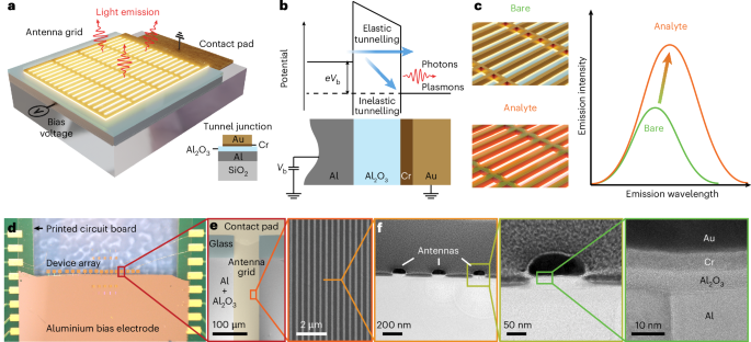
a, Artistic view of the quantum tunnelling-based sensing device. Inset: the layer sequence; doubly periodic Au metasurface with a thin Cr adhesion layer separated by an Al2O3 tunnelling barrier from a 25 nm Al film deposited on a glass substrate. b, Energy-level diagram for the metal–insulator–metal tunnel junction illustrating the possible electron pathways including plasmon/photon emission driven by inelastic tunnelling. c, Illustration of the quantum tunnelling-assisted sensing principle. The bare metasurface (green curve) exhibits a tunnelling luminescence peak that is redshifted and enhanced when the metasurface is covered by an analyte (orange). d, Optical microscope image of an array of devices electrically connected to the metallic pads on a printed circuit board. e, Enlarged optical image from d and SEM image of the metasurface. f, High-resolution TEM image of a thin lamella cut from the metasurface. Further zoom-ins of a single antenna and the tunnelling gap allow us to estimate the thicknesses of the Al2O3 insulator gap (~5 nm) and the Cr adhesion layer (~5 nm).
A schematic of the resulting tunnel junction is shown in Fig. 1b. In the experiments, a positive bias voltage Vb is applied to the Au metasurface layer, while the Al layer is grounded. Inelastic electron tunnelling leads to the excitation of plasmons and subsequent emission of photons that are detected in the far field with a spectrometer system for spectral analysis or with a camera for imaging. To electrically drive the sensor, we utilize a custom-printed circuit board with a set of contact pads (Fig. 1d) that are connected to the pads on the chip via wire bonding. The contact pad of each device is fabricated on top of the bare glass area, while the metasurface extends over the bottom Al contact (Fig. 1e). The transmission electron microscopy (TEM) image of a thin lamella cut from the metasurface in Fig. 1f demonstrates a high-quality tunnelling contact with an Al2O3 barrier thickness of ~5 nm. The proposed design implies no spatial overlap between the analyte on the sensor surface and the emission source (tunnelling gap). While this configuration imposes certain limitations on the sensitivity compared with, for example, picocavity-based sensors9, the transduction of optical signal through the more easily accessible plasmonic lattice mode facilitates analyte handling in practice.
Metasurface electro-optical properties
An important prerequisite for sensing applications is to realize a LIET device that produces highly uniform emission over a large detection area for reliable measurements. Owing to the extreme sensitivity of the tunnel junction to local defects, even minor perturbations along the length of the antennas could lead to voltage drops and strong variations in the emission strength. To illustrate this point, we present in Fig. 2a a metasurface made solely from a 1D array of horizontal nanowire antennas with a period of 400 nm. Its LIET image clearly shows such defect-related emission discontinuities. We mitigate this issue by adding an array of nanowires in the y-axis direction to form an interconnected mesh (see SEM images in Fig. 2b,c). Overall, we observe that the doubly periodic design suppresses discontinuities, but the density of the interconnections also affects the strength of the emission intensity. For example, the LIET image of a high-density mesh with 2D arrays of nanowire having a period of 400 nm in both vertical and horizontal directions in Fig. 2b produces a very low emission yield. Instead, Fig. 2c shows an optimized metasurface with a period of 400 nm and 100 μm in the x- and y-axis directions, respectively. For a quantitative comparison of different designs, we estimate the emission efficiency as the total number of detected photons per tunnelling electron. The colour bar in Fig. 2a–c and the average values indicated on top, obtained from a representative sample set at 2.4 V, provide a comparison for three different designs. For the optimized mesh (Fig. 2c), we detected (0.42 ± 0.21) × 10−7 photons per electron on average over 20 different tested devices, which is ~2.3 times higher than for the square mesh having a period of 400 nm in both vertical and horizontal directions (Fig. 2b). Also, this metasurface design with less interconnections consistently produced a highly uniform emission over a large area with no emission discontinuities in all tested samples. This is a result of a favourable trade-off between the electrical connectivity that improves with a denser mesh and far-field light outcoupling that is facilitated by sparser antennas. Taking into account the possible decay channels for inelastic electron tunnelling, such as SPP leakage radiation into the substrate and emission at larger angles that are not collected within the numerical aperture (NA) of the objective (see Supplementary Section 2.5 for details), we estimate the total conversion efficiency of our device as 1.2 × 10⁻⁷ photons per electron, which is consistent with a theoretical estimate in previous literature37 (1.1 × 10⁻⁷). Although this value is lower than the experimentally reported value37 (1.6 × 10⁻⁶), it is compensated by the design of our device providing uniform emission over large areas.
Fig. 2: Electro-optical characterization of a large-area metasurface.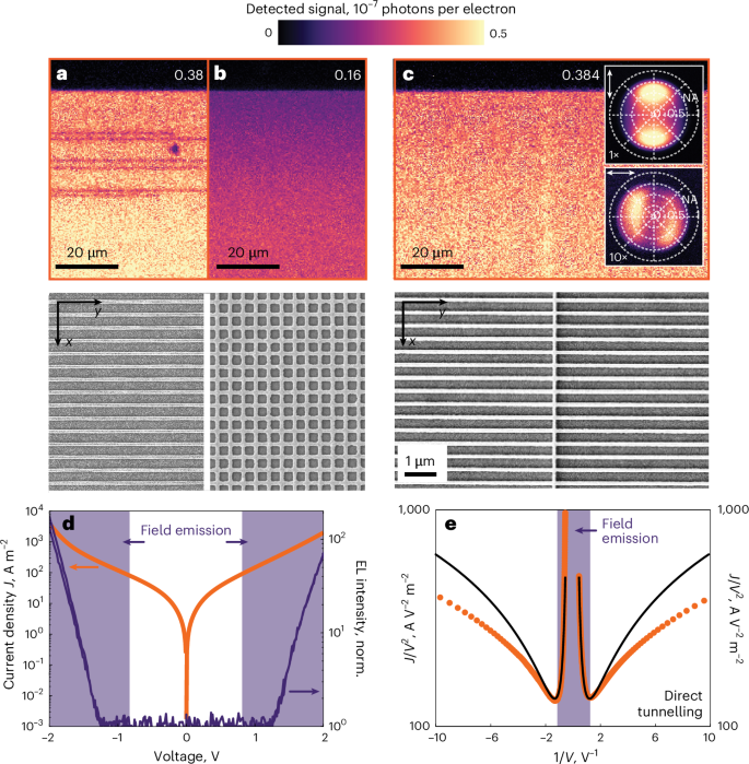
a,b, Top: optical microscope images of the light emission from a metasurface consisting of a 1D array of horizontal nanowires with a period of 400 nm in the vertical direction (a) and a doubly periodic metasurface formed by densely interconnected 2D arrays of nanowires with a period of 400 nm in both directions (b). Bottom: corresponding SEM images. c, Top: image of the spatially homogeneous and electrically stable light emission observed from an optimized doubly periodic metasurface formed by less densely interconnected 2D arrays of nanowires with a 400 nm period in the vertical direction and a 100 μm period in the horizontal direction. Insets: measured angular distributions of the tunnelling luminescence with different orientations of the analyser, illustrating that the observed emission has a dipolar nature. Bottom: SEM image of the optimized metasurface. All measurements in a–c are taken at a voltage of 2.4 V. The numbers in each panel show the average number of photons per electron detected from each structure (in 10−7 units). d, I–V curve (orange) of the optimized metasurface in c along with the simultaneously recorded electroluminescence (EL) intensity from the tunnelling device (dark violet; normalized (norm.) to the noise level of the detector). The range of voltages above the field emission threshold is shaded in light violet. e, Corresponding Fowler–Nordheim representation of the I–V data (orange curve) and its fitting to the Simmons model (black curve). The field emission region (shaded in violet) is clearly defined by the sharp bend of the curve at 0.8 V. Below 0.8 V (above 1.25 in 1/V), the signal is dominated by direct electron tunnelling.
Insets in Fig. 2c present back-focal-plane images of the emission collected from the metasurface for two orthogonal polarizations of the analyser. The radiation patterns show two characteristic lobes that reveal the dipolar nature of the emission associated with the plasmonic mode of the nanowire grid (see Supplementary Section 2.4 for details). The weaker signal with a similar pattern observed for the opposite polarization is consistent with the lower density of nanowire antennas in the orthogonal direction. These observations are supported by calculations of the angle-resolved spectral photonic contribution \({\mathcal{G}}(\omega ,\theta ,\phi )\) (Supplementary Fig. 12).
We further characterize the optimized metasurface through electro-optical measurements. In Fig. 2d, a semilog plot shows the dependence of the current density on the applied bias voltage, exhibiting an exponential profile typical of tunnel junctions37. When the applied voltage exceeds 1.25 V, the light intensity detected by a point photodetector increases linearly with the electric current in the shaded violet area. The transition between direct-tunnelling and field-emission regimes is illustrated in the Fowler–Nordheim representation of the I(V) data in Fig. 2e, which shows a minimum at a voltage of 0.8 V. We fit the I–V data with the Simmons model38, assuming an effective electron mass of 0.23 me (ref. 39). From this analysis, we extract the values of the junction’s mean barrier height φ = 2.62 eV and barrier width Δs = 3.2 nm. The inconsistency of fitting results with TEM data indicates the presence of local (antenna-scale) inhomogeneities of the barrier layer and surface charge phenomena40 that could contribute to diminishing the effective tunnelling barrier width.
We then study the optical properties of LIET by measuring the dependence of the emission spectra on the applied bias voltage. Figure 3a shows the corresponding spectra recorded from the optimized metasurface within the 500–950 nm spectral range for a bias voltage Vb increasing from 1.5 V to 2.3 V. We observe two major trends in the spectra: first, the emission band shifts to shorter wavelengths with increasing Vb, which is explained by the linear change in the cut-off condition with the energy of the emitted photons, ℏωmax = ∣eVb∣ (ref. 37); second, for high enough Vb (>1.9 V), the spectra start to manifest a pronounced peak close to 650 nm. The change of Vb within the 1.5–2.3 V range leads to an increase in the total signal intensity as well as a gradual blueshift of the shorter wavelength peak. At the applied voltage of 2.4 V, the measured emission power density is 0.49 nW mm−2. This brings the total detected power to 40 pW, making our device feasible for use with most standard detectors.
Fig. 3: Experimental and theoretical analysis of the spectral response associated with LIET.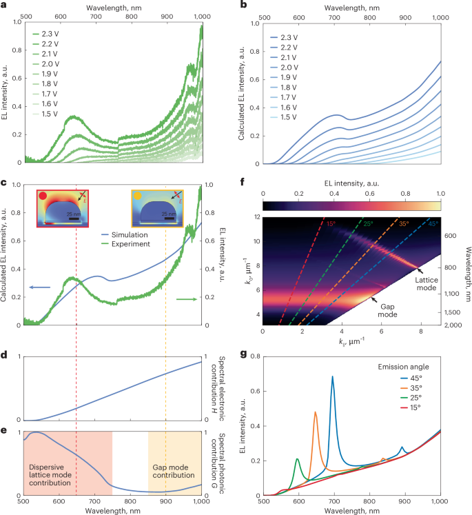
a,b, Electroluminescence spectra of the optimized metasurface for various applied voltages ranging from 1.5 V to 2.3 V as obtained from experimental measurements (a) and theoretical calculations (b). c, Calculated spectrum of emission intensity (blue curve) and its correlation to the experimental emission spectrum (green curve) at Vb = 2.3 V. Insets: the calculated optical electric field amplitude distribution in the x–z plane for p-polarized plane-wave excitation at two characteristic wavelengths under a certain incident polar angle θ: 650 nm (θ = 36°; red line) and 900 nm (θ = 54°; yellow line). d, Calculated normalized spectral electronic contribution H(ω) for Vb = 2.3 V. e, Calculated normalized spectral photonic contribution G(ω). f, Calculated angle-resolved EL intensity in k0 − k∣∣ space. The emission features corresponding to the dispersive plasmonic lattice mode and the dispersionless gap mode are marked with black lines. g, Calculated spectra of emission (solid lines) along a discrete set of angles corresponding to the dashed lines of matching colour in f.
Theoretical model
To elaborate on the origin of the observed spectral features and their evolution with bias voltage, we introduce a theoretical model that describes both the tunnelling process and the antenna-assisted coupling of LIET to the optical far field. The spectrally resolved LIET intensity is calculated as the product of two contributions:
$${I}_{{\rm{LIET}}}(\omega ,{V}_{{\rm{b}}})\propto H(\omega ,{V}_{{\rm{b}}})\times G(\omega ),$$
(1)
where we introduce the spectral electronic contribution H(ω, Vb) across the tunnelling layer as a function of photon frequency ω (that is, the electron energy loss) and applied potential Vb, and the antenna-mediated spectral photonic contribution G(ω) describing the far-field distribution of photons originating from the Al2O3 tunnelling layer. Note that H depends on the overlap between electronic states in the electron emitter and receptor, as well as the gap distance separating them, but it does not depend on the optical properties of the system. By contrast, G encapsulates the optical response, including the far field associated with the transition matrix elements, but it is independent of the electronic matrix elements. Details on the calculations of these two quantities are presented in Methods and Supplementary Information. The results of our simulations closely reproduce the spectral features of the emission observed in the experiment (Fig. 3c) as well as their evolution with increasing Vb (Fig. 3a,b).
Importantly, the model allows us to discriminate between the relative importance of the spectral electronic contribution H(ω, Vb) and the antenna-mediated spectral photonic contribution G(ω) in the resulting spectra. Figure 3d,e shows the spectral dependence of these two functions plotted separately for Vb = 2.3 V. The spectral electronic contribution H(ω, Vb) has no pronounced spectral features (Fig. 3d) and its effect on the total emission intensity is a gradual increase towards longer wavelengths. By contrast, G(ω) (Fig. 3e) exhibits spectral variations associated with the optical modes excited in the structure. The enhancement of G(ω) in the spectral range from 500 nm to 750 nm originates from the dispersive plasmonic lattice mode. To illustrate this, in Fig. 3f, we plot the calculated angle-resolved emission. The plasmonic lattice mode manifests as an angle-dependent emission peak spanning the range of wave vector k between 8 μm−1 and 11 μm−1. The emission spectra at a discrete set of angles indicated with dashed lines in Fig. 3f are shown in Fig. 3g. The combined contribution of the electronic component H(ω, Vb) and the photonic component G(ω) averaged over the angular range corresponding to the NA of the collection objective leads to the formation of the main feature in the total emission (that is, the peak at ~650 nm). This is further detailed in Supplementary Fig. 10 and the related discussion in Supplementary Section 2.3. The angle-resolved spectra also reveal the emission associated with the dispersionless plasmonic gap mode manifested as a peak at around 1,000 nm. Notably, while the Cr layer quenches the contribution from the plasmonic gap mode in the photonic part G (Supplementary Figs. 8 and 9), this layer has a positive influence on the total electroluminescence intensity. This is partly due to substantially higher values of the spectral electronic contribution H from better matching between the electric band structures of Cr and Al.
Additional simulations of the electric near field of the nanoantenna shown in the insets of Fig. 3c further support the assignment of spectral features of emission to the plasmonic lattice mode and the gap mode. The electric near-field map calculated for p-polarized plane-wave excitation at 650 nm (Fig. 3c, inset in red box) shows two characteristic hotspots at the top surface of the antenna. The minor increase in G(ω) at longer wavelengths (>850 nm) represents the contribution from the plasmonic gap mode, which has its resonant frequency outside of the spectral range of detection (Supplementary Fig. 11). Accordingly, the near-field distribution for plane-wave excitation at 900 nm (Fig. 3c, inset in yellow box) reveals a maximum field in the Al2O3 insulating layer.
Biosensing with a self-illuminating metasurface
To benchmark the on-chip LIET-based optical biosensor, we test it with two organic analytes using a polymethyl methacrylate (PMMA) polymer layer and a thin film of amino acid biomolecules. Figure 4a shows the LIET image of the metasurface covered with 45-nm-thick PMMA and biased at 2.8 V. To illustrate the changes in the emission intensity and the spectrum with and without analyte, after spin-coating a uniform layer of PMMA on the sensor surface, we use electron-beam (e-beam) exposure and subsequent development steps to selectively remove the polymer and create PMMA-free regions. Figure 4a shows a rectangularly shaped bare region (green box) that is used for reference spectra measurements as well as a patterned region in the form of the EPFL logo (orange box). The image shows a 2.2-fold enhancement of the emission intensity at ~650 nm on the areas covered with the analyte film compared with the bare regions, and the intensity distribution remains spatially uniform. Further insight is provided by the emission spectra shown in Fig. 4b, which are measured from the bare (green curve) and analyte-covered (orange curve) regions of interest on the functionalized LIET device. The spectra reveal that the stronger emission intensity in the LIET image is mainly due to enhancement of the shorter wavelength peak corresponding to the dipolar plasmon mode of the nanowire antenna.
Fig. 4: Demonstration of label-free biosensing by LIET in optimized metasurfaces.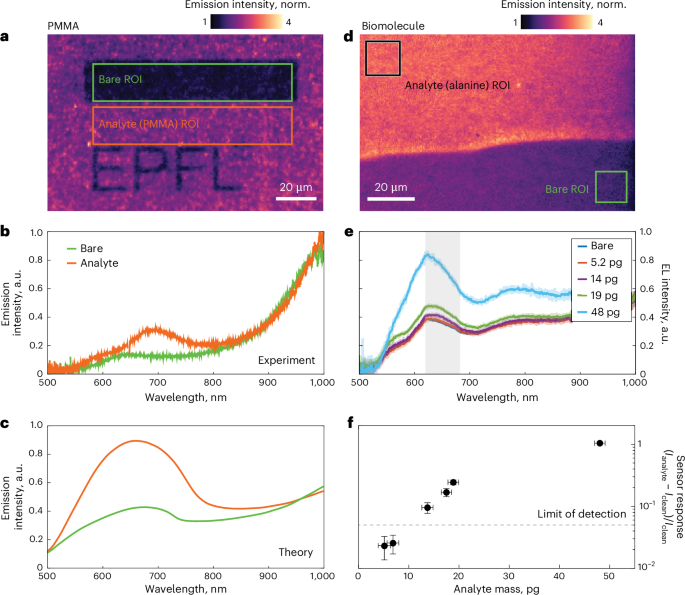
a, Image of the homogeneous light emission from the optimized metasurface with (orange box, analyte region of interest (ROI)) and without (green box, bare ROI) a coating PMMA thin film. b, Spectral response from the colour-matched regions in a: orange/green with/without PMMA. c, Simulated electroluminescence spectra under the conditions of b. d, Image of light emission from a metasurface partially covered with alanine (black box, analyte ROI) and without alanine (green box, bare ROI). e, LIET electroluminescence spectra measured for different amounts of alanine evaporated on the sensor surface. The semitransparent curves show the raw data, while the solid curves show the data smoothed over a window of 2.5 nm (10 points). f, Sensor response for different amounts of alanine extracted as a differential emission signal averaged within the 620–700 nm spectral range, highlighted in grey in e, with two additional data points at 7 pg and 18 pg. The limit of detection defined as triple the noise level is indicated by a dashed line. The sensor responses are presented as mean values for three samples ± s.d., where s.d. stands for standard deviation from the statistical uncertainty. Alanine thicknesses are presented as mean values ± s.d. derived from AFM measurements.
To elaborate on the origin of the changes in the emission owing to the presence of a PMMA film, we considered a uniform layer with a thickness of 45 nm and a refractive index of 1.49 (ref. 41) in the theoretical model used above. The modifications of the spectra observed in the experiment are in good agreement with our simulations based on equation (1) (Fig. 4c). The dominant effect is an increase in the amplitude of the ~650 nm peak, which is well reproduced in the simulations (2.13-fold increase versus 2.2 in the experiment). This intensity change originates from the refractometric spectral redshift of the dispersive plasmonic lattice mode, which improves the coupling of emission into the NA of the objective (see Supplementary Fig. 13 and detailed discussion in Supplementary Section 2.4).
Finally, to demonstrate the biosensing application of our device and quantitatively estimate the sensitivity performance, we studied the dependence of the LIET signal on varying amounts of biomolecules deposited on the surface of the device. For these studies, the antenna width of the sample was slightly changed from 92.5 nm to 120 nm. This new width did not lead to any sizable changes in the spectral profile (Fig. 4b,e), but allowed us to use a 10× (NA = 0.3) objective lens owing to the shift in the dispersion of plasmonic lattice modes towards small angles. In this way, we were able to compare the sensing performance with a state-of-the-art plasmonic biosensor based on Au nanohole arrays that are optimized for low NA optics. As a bioanalyte, we used alanine, which is an α-amino acid with the chemical formula C3H7NO2 and a molecular weight of 89 daltons. Small amounts of alanine were deposited onto the sample surface through thermal evaporation. During the evaporation process, we used a shadow mask to block a portion of the structure, creating an uncovered region with a well-defined boundary that served as an in-line reference (see Supplementary Section 1.2 for details). Figure 4d shows a LIET image of the sensor surface partially covered with alanine. Similar to the PMMA data shown in Fig. 4a, the analyte-covered region exhibits an increase in the LIET intensity. To test the limit of detection of our sensor, we performed measurements for different amounts of biomolecules ranging from ~5 pg to ~50 pg (see Supplementary Section 1.2 for an estimation of the analyte amount). Figure 4e shows the response of the sensor to different doses of evaporated analyte, indicating a gradual increase in the detected emission intensity for higher amounts of alanine. As an output metric for our sensor, we used the LIET intensity. This holds several advantages over spectral shift characterization, namely simpler detection principle, higher signal-to-noise ratio and faster response time. We integrated the emission within a spectral region from 620 nm to 700 nm because this yielded the strongest modulation in the LIET signal, which in practice can be realized by introducing a spectral band-pass filter in the detection scheme. The extracted data are plotted in Fig. 4f, normalized to the integrated emission of the bare chip. Our measurements indicate a reliable detection of analyte down to ~9 pg within the signal collection area, defined as a mass for which the response of the sensor is 3 times larger than the noise level. To correlate the performance of our device with state-of-the-art methods, we used an optimized nanoplasmonic biosensor consisting of Au nanohole arrays with 630 nm RIU−1 of bulk sensitivity42, which is well within the range reported in the literature43 (see Supplementary Section 1.2 for details). The results show a similar signal amplitude, highlighting the potential of our LIET platform for high-performance biosensing.