In the following we discuss a minimal model to account for our key observations: (i) the formation of a large SpV that (ii) can drive a persistent electric current across an external circuit, that (iii) develops gradually below about 120 K, more or less in parallel with the FM order (at \(B\) ≈ 0), that (iv) increases in magnitude towards low temperature, that (v) undergoes sudden changes of the magnitude and even the sign during temperature-sweeps and magnetic field (\(H\)) loops, that (vi) exists in zero magnetic field with even symmetry under time reversal (magnetic field), and that (vii) exhibits clear hysteresis and memory effects during field sweeps.
At first, we emphasize that the above-described features are incompatible with a thermoelectric effect that arises from a thermal gradient across the YBCO/NCSMO heterostructure or the wires connected to it. Such a scenario could not explain the persistence of the SpV signal and the related currents, since the sample is glued to the cold finger of the cryostat and thus strongly coupled to a heat bath. Accordingly, the thermal gradient would depend on the cooling rate and decrease over time while the sample is dwelling at a fixed temperature. Moreover, the typical magnitude of such a thermoelectric voltage is on the order of microvolts, rather than millivolts, and it has a maximum at elevated temperatures and decreases strongly towards low temperature (see Supplementary Note 2). Finally, a thermoelectric voltage is not expected to undergo jump-like changes during temperature and magnetic field loops nor to exhibit a memory effect. For the reasons described above, we can exclude any alternative mechanism for which the energy that is required to develop a SpV and drive a persistent electric current through an external circuit is drawn from an external heat bath. Here the ubiquitous decrease of the lattice contribution to the thermal conductivity and the heat capacity would cause a strong reduction of the energy transfer at low temperature, and as a consequence also of the SpV.
In the following, we argue instead that a rectification of electronic noise based on an asymmetric, ratchet-like electronic potential is at the heart of the SpV and the persistent current effects that require a steady-state generation of power. Here, the device acts as the receiver and the source of energy is provided by the environmental electronic fluctuations/noise that the sample is exposed to inside the magneto-cryostat of the physical property measurement system (PPMS). As detailed in the Supplementary Note 3, we have verified that the SpV signal is sensitive to the change of the driving mode of the PPMS magnet, as well as to electromagnetic radiation created with an a.c. current generator which is connected to a coil that is located inside the PPMS sample chamber (Supplementary Note 4). Moreover, in corresponding a.c. transport measurements, we detected a 2nd harmonic signal that develops in parallel with the SpV below about 120 K and increases in magnitude towards low temperature (see Supplementary Note 5).
We argue that the ratchet-type electronic potential has its origin in the complex domain state of the NCSMO layers. The manganites are indeed known for their rich spectrum of magnetic and electronic orders that results from the competition between the superexchange, double exchange and Jahn-Teller interactions. A famous example is the colossal magnetoresistance (CMR) effect which occurs e.g. in La1-x(Ca,Sr)xMnO3 with 0.2 19,20,21. Equally intriguing phase competition phenomena occur for the systems with more strongly tilted Mn-O-Mn bonds, e.g. in (Pr,Nd)1-x(Ca,Sr)xMnO3 with 0.3 22 that are either long-range ordered, and give rise to a phase with charge-exchange-type AF and charge/orbital order (AF-COO), or they are in a disordered “liquid-like” state (D-phase).
Notably, the distorted Mn-O-Mn bonds in the AF-COO state give rise to a polar electric moment and a subsequent domain state with charged domain walls22 (See Supplementary Note 1). The reported size of these polar domains is about 20 nm, the polar moments are directed along the \(a\)-axis and cause head-to-head or tail-to-tail domain walls whose normal vectors are along the polar moments22. The estimated values of the net polarization and the dielectric constant of \(P\) ≈ 40 mC/\({{{\rm{m}}}}^{2}\) and \({\varepsilon }\) ≈35, respectively, yield a sizeable change of the electric potential of ~2 V between the opposite types of domain walls and an electric field strength of \(E\,{\approx }\,{10}^{8}\) V/m. The corresponding surface charge density of the domain walls amounts to about \({{\rm{\pm }}}0.07\) electrons per pseudocubic u.c. of NCSMO (see Supplementary Note 4 for more details).
The transition to this charge/orbital ordered and polar state occurs around \({T}_{{COO}}\) ≈ 230–250 K, depending on the composition and doping level21,23. It appears to be of an order-disorder type with a gradually increasing volume fraction of the COO phase towards low temperature22. The magnetic transition of the AF phase occurs around \({T}^{N}\)≈ 140–170 K24. An additional FM transition occurs in the range of \({T}^{{Curie}}\) ≈ 110–130 K20 in zero or low magnetic fields. Here the magnetic moment and thus the volume fraction of this FM phase amounts to less than 10% of that in the bulk FM state of e.g. La2/3Sr1/3MnO3 with a saturation value of about 3.7 \({{\mu }}_{B}\)/Mn21. Whether this FM minority phase develops merely at the expense of the AF-COO phase or also of the D-phase is unknown. There exists, however, clear evidence of a strong competition between the FM and the AF-COO phases. For example, the FM moment and the related volume fraction can be strongly enhanced with a large external field that tips the balance between the competing AF-COO and FM phases towards the latter. Similar changes can be induced with other external stimuli, like electric currents22 or high energy photons25,26.
In the following, we propose a minimal model to account for the SpV and its unusual temperature and magnetic field dependence, that is based on a ratchet-type potential that arises from the competition between the polar COO phase and the non-polar FM phase and their pinning-induced inhomogeneous lateral distribution. Figure 7a shows a sketch of the electronic potential for a balanced polar domain configuration with a vanishing total polar moment (\(\langle p\rangle\)=0) that minimizes the energy due to electric stray fields and occurs at elevated temperatures where the FM phase is absent, i.e. at T > TCurie. For simplicity, the sketch does not show the coexisting non-polar D-phase, which is likely segregated from the polar COO phase, see e.g. ref. 19. The sketch in Fig. 7b shows how the electric potential of this compensated polar domain state is modified when the nonpolar FM phase appears at T Curie and starts to compete with the polar AF-COO phase. Here we assume that the nonpolar FM phase develops right at the head-to-head domain walls for which the electric potential is maximal and thus attractive for electrons. Such a scenario is suggested by the doping phase diagram of the manganites where the FM phase (AF-COO phase) prevails at lower (higher) hole doping20,21. Figure 7b shows that the non-polar FM phase gives rise to a reduction of the electronic potential in its vicinity. It also reveals that a spatially inhomogeneous distribution of these non-polar FM domains causes an asymmetry of the electronic potential and subsequently a SpV between contacts that cover regions with a different density of the FM patches (note that the sketch is not to scale with respect to the size of the contacts and the polar domains). Such an inhomogeneous distribution of the FM phase is likely caused by a pinning to local or extended defects that exhibit a density gradient across the sample. Such a lateral gradient may arise e.g. from a terrace structure due to an imperfect surface cut of the substrate27, from a long-ranged strain gradient across the sample due to the lattice mismatch between the substrate and the thin film28, or from a lateral variation of the chemical composition of the thin film that is inherent to the PLD growth process, due to the complexity of the ionic composition and dynamics of the plasma plume29.
Fig. 7: Illustration of the origin of the SpV from competing polar AF-COO and non-polar FM phases.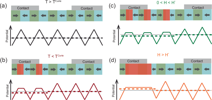
a Electronic potential for a compensated polar domain state (\(\left\langle {{\rm{p}}}\right\rangle\) = 0) of the bare AF-COO phase at \({T}^{{Curie}} . The electronic potential, Φ, and its average over pairs of neighboring polar domains, \(\left\langle \Phi \right\rangle\), are shown by solid and dashed lines, respectively. The green and cyan regions indicate regions with opposite polarity, where the arrows correspond to their polar moment. b Reduction of Φ in regions where the non-polar FM domains (red coloring) develop at the polar head-to-head boundaries. c Sudden change of the electronic potential upon increasing H-field. Below the threshold field \(H the non-polar FM domains develop around individual head-to-head boundaries where they reduce Φ. d Above \({H}^{*}\) the FM domains start to cluster and cover extended regions giving rise to a sudden increase of 〈Φ〉.
The occurrence of a large SpV signal furthermore requires that the volume fraction of the non-polar FM- and D-phases remains below the percolation limit, above which conducting pathways develop across the multilayer that can short the contacts. It is equally important that the YBCO layers are rather thin such that they can only partially screen the electric fields that emanate from the charged domain walls. The charge carriers of the YBCO layers are thus localized in the vicinity of the polar COO phase and remain mobile only in the regions of the non-polar FM- and D-phases. A percolation effect due to a growing fraction of the nonpolar D-phase, in combination with the suppression of the FM order above \({T}^{{Curie}}\), therefore can explain the strong reduction of the SpV signal above 120 K. Likewise, the reduction of the SpV signal by a large magnetic field (at \({T} ) can be readily understood in terms of an enhanced volume fraction of the nonpolar FM phase.
Next, we show that the above-described minimal model may also account for the sudden changes of the magnitude and even the sign of the SpV that occur in the experimental field loops in Fig. 3c, d. The sketches in Fig. 7c, d show that a sudden change of the electronic potential landscape \(\Phi\) can occur as the volume fraction of the nonpolar FM regions increases and they eventually start to merge forming extended clusters. Note that above a certain threshold field value \({H}^{*}\) such a clustering can be energetically favorable, since it enhances the electronic potential in the vicinity of the FM phase (as compared to the case where the FM patches are confined to single domain walls). Moreover, the FM clusters might be forming extended conglomerates for which a switching between different ordering patterns can be induced with a magnetic field. The memory effect of the SpV signal can arise here because the various ordering patterns are preset by the spatial distribution of the underlying pinning centers (due to the defects discussed above). Such a scenario also seems consistent with the finding that the large and sudden changes of the SpV signal occur only at elevated temperatures, i.e. between about 40 K and 80 K, where the thermal energy helps to overcome the energy barriers between the various energetically favorable patterns and the SpV signal thus becomes reversible.
The minimal model shown in Fig. 7 is also compatible with the almost symmetric shape of the magnetic field loops of the SpV signal for which the magnitude and sign are independent of the direction of the applied field. Here, the magnetic field changes the energy balance between the competing AF-COO and FM phases by an amount that is proportional to the magnetization squared30 and thus independent of the sign of the field.
Finally, we further discuss the role played by the YBCO layers, which enable the lateral charge flow and thus are essential for using the SpV to drive a persistent current across an external circuit. These YBCO layers are fully oxygenated and thus close to optimal hole doping. Their superconducting (SC) transition temperatures of \({T}_{c}\) ≈ 70–80 K are indeed only moderately reduced as compared to the bulk value of \({T}_{c}\) ≈ 90 K31,32. However, despite a robust SC pairing strength, the macroscopic SC phase coherence of these YBCO layers appears to be very fragile, similar to granular superconductors16,33.
A finite SpV signal only occurs as long as the thickness of the YBCO layer remains below the screening length, \({l}^{{sc}}\), (introduced in Fig. 6) such that it can only partially screen the electric field that emerges from the charged boundaries of the polar COO domains in the neighboring NCSMO layers. Moreover, it is mandatory that the NCSMO layers contain a sufficiently low fraction of the nonpolar FM or D-phases as to avoid the formation of conducting pathways across the YBCO layers. The charge carriers of the YBCO layers are thus weakly localized. However, they can be activated by absorbing photons from the background radiation, which enables them to overcome the barriers of the partially screened ratchet-type potential and develop a lateral charge flow. This interpretation agrees with our finding that a corresponding persistent current effect does not occur for a single NCSMO layer, as shown in the Supplementary Note 6. It is also confirmed by the variation of the SpV signal as a function of the thickness of the YBCO layer shown in Fig. 6 which exhibits the expected exponential trend, \({Sp}{V}_{\max } \sim A.\exp (-d/2{l}^{{sc}})\) with \({l}^{{sc}}\) ≈ 4.7 nm. This value is quite a bit larger than the estimated Thomas-Fermi-screening length of about 0.1 nm34 (given the carrier density of optimal doped YBCO35 of ~1021 holes/cm3). The enhanced screening length may result from the quasi-two-dimensional structure of YBCO, even though, corresponding Thomas-Fermi-theory based calculations suggest that a particle with an elementary charge \({e}^{-}\) is almost fully screened by a single CuO2 plane36. Nevertheless, in these calculations it is not considered that the high-Tc cuprates are hole doped Mott-insulators which have a rather limited capacity for screening positive charges. This is especially true for the interfacial CuO2 layers for which the hole doping is reduced by a charge transfer across the interface37 as well as by the absence of a CuO chain layer (and thus charge reservoir) right at the interface38,39.
To summarize, our study has identified YBCO/NCSMO multilayers as promising artificial materials for creating devices for efficient energy harvesting of electronic background noise. In particular, we have shown that they can develop rather large SpV signals on the order of tens of millivolts in a wide range of temperatures and magnetic fields. We have also demonstrated that this SpV can drive a persistent current through an external circuit and thus perform electrical work. Moreover, we have found that the magnetic field loops of the SpV signal exhibit pronounced hysteresis and memory effects which can be readily modified via the temperature and applied electric currents, and most likely also electromagnetic radiation40,41,42. These YBCO/NCSMO multilayers thus provide opportunities for developing self-powered multifunctional devices and non-volatile memories.
We emphasize that our results are distinguished from previous work43,44,45,46 on zero-field non-reciprocal transport since we observe large SpV and SpC effects over a temperature range of more than 100 K. Moreover, a SpV signal with even-in-field symmetry, to our best knowledge, was only reported for disordered Nb channels and thin films47 where a SpV at zero-field appears only in a narrow temperature window around Tc ~ 3 K.
Our study is also of great interest from a fundamental science perspective. In the first place, it has highlighted the complexity of the domain state of the NCSMO layers which in addition to various orbital and magnetic orders give rise to a polar order of the COO phase and a subsequent charging of domain walls, which has so far received limited attention. Our study has also revealed an important role of the YBCO layers which are nominally metallic and superconducting. In particular, it has provided evidence for a rather large length scale (\({l}^{{sc}}\) ≈ 4.7 nm) of the screening of the electric fields that emanate from the charged domain boundaries of the neighboring NCSMO layers. This finding has direct implications for electric field-effect studies in related heterostructures with thin superconducting layers of high-Tc cuprates, for which the direct interaction of the static electric field with the superconducting order parameter has been widely neglected but is recently obtaining increased attention48,49,50,51,52,53,54.
Our findings also indicate a possible correlation between the onset below 80 K of the superconductivity in the YBCO layers and the strong enhancement and large fluctuations of the SpV. Such a coincidence could imply a back-action of the superconducting order in YBCO on the domain state of the neighboring NCSMO layers. Such a cross-talk might be mediated by the interaction of the vortices of the SC with the FM domains. Likewise, it could be related to the poor screening capability of the YBCO for positive charges (due to the above discussed proximity to a Mott-insulator state) and the subsequent formation of a pattern of alternating SC and insulating domains in the YBCO layer. Such a domain state could act like a network of Josephson-type junctions and thus contribute to the sudden changes of the magnetic field loops in Fig. 3 and their pronounced memory effects.
Microscopic scanning probe studies of the structure of the complex domain state of these YBCO/NCSMO heterostructures will be required in order to fully understand the mechanism underlying their SpV and SpC effects. It will also be of great interest to explore whether defect or strain engineering can be used to further enhance the amplitude and control the sign of the SpV and SpC signals and to tailor the pronounced hysteresis and switching effects in the temperature and \(H\)-field loops. Likewise, it remains to be further explored how the SpV and SpC signals depend on the polarization, spectral distribution and intensity of the electromagnetic background radiation, as well on the size and shape of the electric contacts of the samples.