Design and linear characterization
Figure 1 illustrates the design and working principle of our device. We investigate a nonlocal lithium niobate on insulator (LNOI) metasurface made by asymmetric, periodically arranged nanostripes obtained from an x-cut LiNbO3 thin film on a finite SiO2 layer on top of a Si substrate (Fig. 1a). We aim at observing efficient and fast electric modulation of the metasurface optical properties induced by a control voltage, VEO applied to the metasurface. To this aim, in-plane, gold contacts generate an electric field (EEO) aligned along the z-axis to exploit the largest component of the electro-optic tensor r33 of LiNbO3. To obtain a significant intensity modulation, the structure must sustain resonant modes, which are spectrally shifted when the refractive index is modulated by an applied voltage (Fig. 1b). Furthermore, at a given wavelength λ0, a device with large quality factor Q = λ0/δλ0 features a resonance with a narrow spectral width δλ0 and, consequently, a large sensitivity to small variations of the refractive index induced by the applied voltage.
Fig. 1: Linear and nonlinear electro-optic modulation with a lithium niobate metasurface.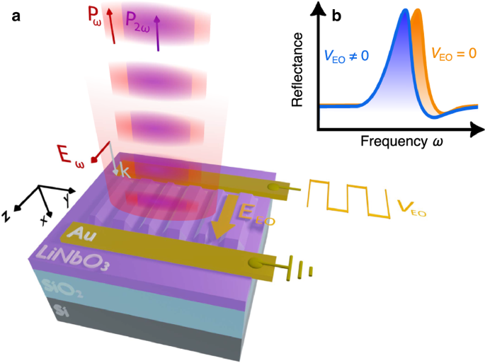
a Sketch of modulated reflected power of a beam at fundamental frequency \({P}_{\omega }\) and of its second harmonic \({P}_{2\omega }\) from a x-cut LiNbO3 on a SiO2-Si substrate. The modulation is induced by an applied voltage (VEO), which produces a driving electric field EEO parallel to the optical field Eω. b Illustration of a resonance shift induced by electro-optic effect.
To this aim, we exploit high Q resonances hosted by a dielectric waveguide slab − namely, a high refractive index layer (LiNbO3), comprised between two low-index claddings (air and SiO2)—patterned with periodically arranged nanowires (i.e. a diffraction grating)34. Figure 2a shows a sketch of the elementary cell of the metasurface with the relevant geometrical parameters. A planar dielectric waveguide is known to host guided modes whose dispersion lies below the light line, fully confining the radiation in the slab volume with no access from external radiation sources. The reduction of translational symmetry introduced by the grating causes a folding of the guided modes dispersion in the first Brillouin zone, ending up above the light line, and consequently evolving in optically accessible guided mode resonances (GMRs)34,35. A mirror symmetry of the grating with respect to the xz plane yields a dark fundamental mode at the Γ point (i.e., at normal incidence) due to the odd electric field distribution (see Fig. 2b), namely becoming a symmetry-protected BIC. By introducing a small asymmetry in the nanowires’ widths, we further reduce the translational symmetry of the system, turning the BIC into a leaky, quasi-BIC with finite Q (see Fig. 2c), which can now be excited at the Γ point.
Fig. 2: Sample layout and linear optical characterization.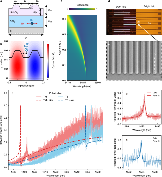
a Schematic cross-section of a single unit cell of the metasurface. All the samples have the same periodicity p = 800 nm and LiNbO3 height before (hLN = 600 nm) and after patterning (h’LN = 450 nm) with a substrate thickness, hsub = 2 μm. The angle θ = 65° accounts for the sidewall slopes introduced by the physical etching. The variable parameters from sample to sample are the filling factor \(\left.{FF}=1-({D}_{1}\,+{D}_{2})/p\right)\) and the asymmetry parameter \(\alpha=({D}_{2}-{D}_{1})/({D}_{2}+{D}_{1})\). Red and blue arrows indicate the polarization of the incident wave that excites the TM (parallel to the LN ordinary axis) and TE (parallel to the LN extraordinary axis) mode, respectively. b COMSOL simulation of the optical field z-component of the optical field Eopt, excited at the quasi-BIC resonance for FF = 0.3 and α = 0. Incident optical field Eopt is TE-polarized and propagates with k || (–x). c COMSOL plane-wave simulation of the metasurface reflectance depending on the asymmetry parameter \(\alpha\), with fixed FF = 0.3. d Dark field and bright-field images in real colours of the LiNbO3 chip. The LiNbO3 metasurfaces are located in the areas with strong scattering (bright areas in dark field). The white scale bar on the bottom right is equal to 100 μm. The orange lines in the bright field image identify the edges of the interdigitated electrodes. e Scanning-electron micrograph showing the metasurface obtained by patterning the LiNbO3 thin film. The scale bar on the bottom right is equal to 500 nm. The white, dashed line indicates the LiNbO3 extraordinary axis. f Normalized reflection spectra of the sample with FF = 0.3 and α = 0.19. The solid lines show experimental data obtained by sweeping the laser wavelength in steps of 10 p.m., with electric field exciting the TE (blue solid line) and TM (red solid line) mode. The dashed lines are the corresponding numerical simulations. g, h Zoom on spectra shown in panel f (thin lines) fitted with Fano profiles (thick lines) for TM and TE polarization, respectively.
The design optimization has been performed initially by means of rigorous coupled-wave analysis, typically applied to solve scattering from periodic dielectric structures36. The EO effect and the SHG are then modelled with a finite-element commercial software (COMSOL Multiphysics®, see Methods and Supplementary Information S2). By setting the unit cell periodicity as p = 800 nm (see Fig. 2a), the metasurface features the fundamental TE21 resonant mode at the Γ point in the communication C band (i.e, 1530 to 1565 nm). This mode shows up in the reflectance spectrum when the structure asymmetry \(\alpha=\,({D}_{2}-\,{D}_{1})/\,({D}_{2}\,+\,{D}_{1})\) is nonzero, with a linewidth broadening with increasing α (see Fig. 2c)37. We set \({D}_{1}\) and \({D}_{2}\) to have a fill factor \({FF}=1-({D}_{1}\,+{D}_{2})/p=0.3\), corresponding to a fundamental TE mode around 1550 nm, and α = 0.2, to realize a theoretical Q = 11000. Such a value for the Q factor is selected since it allows more tolerance in terms of fabrication accuracy and better resonance coupling in the experiment. Nevertheless, Q is sufficiently high to achieve efficient EO modulation, since the associated mode linewidth (δλ0 \(\simeq\) 0.15 nm) is comparable with the expected EO shift induced by CMOS-compatible voltages, assuming a tuning sensitivity ΔλEO/ΔVEO \(\approx\) 0.01 nm/V28,30.
The metasurfaces were realized on a commercial LNOI stack with 600 nm-thick LiNbO3 film on top of a SiO2 layer with thickness hsub = 2 μm (see Fig. 2d, e) following a top-down approach (see Methods and ref. 38). The choice of planar Au electrodes ensures a uniform distribution of the driving electric field in the LiNbO3 film (see Fig. S3, Supplementary Information), which increases the overlap with the field of the optical mode, also located mostly in the LiNbO3 volume (see Fig. 2b). The uniform electric field distribution is advantageous for electro-optic (EO) modulation, as effectively leveraging the Pockels effect depends on the overlap between the low-frequency electric field and the optical field within the LiNbO3 material. The elongated footprint of the metasurface ensures a large active area to fully exploit the high Q of the nonlocal mode, which extends in the direction where the translational symmetry breaking occurs. On the other hand, the metasurface width is reduced to 10 μm to increase the driving field amplitude. Concurrently, the large electrode width minimizes the contact resistance, hence reducing the impact on the device bandwidth. We realized a set of replicas with slight variation of D1 and D2 (see Methods for details and Supplementary Information S3) to target the sample geometry closer to the desired quality factor and resonance position, finally identifying a fabricated replica with α = 0.19 and FF = 0.3 as the one matching the original design specifications. Additionally, to demonstrate the generality of this approach, we also investigated a sample with FF = 0.5, which is characterized by a fundamental mode around 1560 nm (see Supplementary Information, sections S3 and S6).
The linear properties and the EO response of the sample are characterized in an epi-reflection configuration by impinging with a linearly polarized, continuous-wave (CW) diode laser tuneable in the optical communication C band (1460 nm–1570 nm) and detecting the reflected signal with a photodiode (details in Methods and Supplementary Information S1). The quasi-BIC resonance wavelength shifts when interrogated away from the Γ point of the photonic band structure, typically by about 10 nm/deg. Therefore, to mitigate the resonance linewidth broadening resulting from the angular spread of the light from the objective, we use a cylindrical lens to focus the excitation beam onto the objective back-aperture. This approach effectively reduces the numerical aperture, enabling nearly collimated illumination in the direction of the nonlocal mode extension. At the same time, due to the one-dimensional character of the metasurface, we tightly focus the beam on the direction parallel to the nanowires, hence preserving a sizeable beam fluence (see Supplementary Information, Fig. S1a). We determine the resonance position by sweeping the laser wavelength, obtaining the reflectance spectra depicted in Fig. 2f. The sharp quasi-BIC peak is superimposed to a broad Fabry–Pérot fringe caused by the 2 μm-thick SiO2 layer. A polarization parallel or perpendicular with respect to the LiNbO3 extraordinary index ne excites either a transverse-electric (TE) or transverse-magnetic (TM) mode, respectively, resulting in a reflection peak at 1553 nm or 1492 nm, respectively. We also report an experimental redshift of about 5 nm with respect to the COMSOL finite-element simulations of the same structures (see Fig. 2f). This slight discrepancy could be attributed to deviations of the fabricated nanostructure from its nominal design. Due to the asymmetry in the resonance lineshape arising from the interaction between the sharp quasi-BIC and the broad Fabry-Perot fringe, we fitted the experimental data using a Fano profile (see Fig. 2g, h)39. We evaluate the resonance quality factor of the TE mode Qexp to be larger than 7500, where \(\delta {\lambda }_{0}^{\exp }\,\)≃0.20 nm is the resonance linewidth retrieved from the fitting. This result is in good agreement with the value calculated from the simulations (Qsim \(\simeq\) 11000 with \(\delta {\lambda }_{0}^{{{\rm{sim}}}}\) = 0.15 nm). The lower value of Qexp with respect to Qsim might be related to fabrication tolerances and to the difference in excitation between the simulated platform (perfectly planar wavefront) and the real system (partially collimated beam).
We investigate the static EO response of the device by applying a bias VEO = VDC by means of a waveform generator. The shift of the quasi-BIC resonance can be clearly identified in the reflectance spectra of Fig. 3a, superimposed to an unmodulated instrumental artifact. From the central wavelength λ0, retrieved by the Fano fit, we estimate an EO induced shift of about ΔλEO \(\simeq\) 0.05 nm when ΔVDC = 9 V, close to the value retrieved from the simulated spectra in Fig. 3d (\(\Delta {\lambda }_{{{\rm{EO}}}}^{{{\rm{sim}}}}\simeq\) 0.06 nm). We, therefore, estimate a device tuning sensitivity \(\Delta {\lambda }_{{{\rm{EO}}}}/\Delta {V}_{{{\rm{EO}}}}\) = 5.6 pm/V. To observe the dynamic modulation of the reflectance, we apply a sinusoidal driving potential \({V}_{{{\rm{EO}}}}\left(t\right)\,=\,\frac{{V}_{{{\rm{pp}}}}}{2}\sin \left(2\pi {f}_{{\mathrm{mod}}}t\right)\), characterized by a variable peak-to-peak amplitude Vpp and modulation frequency fmod. We use a lock-in amplifier, referenced by the same waveform generator, to demodulate at f = fmod, obtaining the signal oscillation amplitude \({P}_{\omega }\left(f={f}_{{\mathrm{mod}}}\right).\) The DC component of the signal \({P}_{\omega }\left(f=0\right)\) (namely, the reflectance) is synchronously detected in order to track modulation efficiency variations while changing excitation wavelength. We modulate the signal at fmod = 100 kHz, well below the cutoff of our detection system (600 MHz). The relative modulation is calculated by evaluating the ratio \({P}_{\omega }(f={f}_{{\mathrm{mod}}})/{P}_{\omega }\left(f=0\right)\), which corresponds to \(\Delta {P}_{\omega }/\,{P}_{\omega }=({P}_{\omega }(V={V}_{{{\rm{pp}}}}/\,2)-{P}_{\omega }(V=0))/{P}_{\omega }(V=0)\). The dispersive nature of the reflection spectrum will cause a dependence on λ of the modulation amplitude, which is maximized by exciting at the resonance derivative extrema. The maximum modulation amplitude that is obtained from the data in Fig. 3b is \(\varDelta {P}_{{\it{\omega }}}/{P}_{{\it{\omega }}}\cong 0.12\) (i.e., 0.24 of peak-to-peak relative modulation), obtained with an input voltage as low as Vpp = 20 V. This is approximately 5 times smaller than the value obtained from simulations (see Fig. 3e). Such a discrepancy is mostly ascribed to two experimental limitations. On the one hand, the experimental reflectance background is larger than the simulated one (see Fig. 2f), hence reducing the resonance contrast and, consequently, the relative modulation. On the other hand, the presence of fabrication tolerances (e.g., periodicity, asymmetry) and defects in the realized sample, as well as deviations from ideal plane-wave illumination, both contribute to the reduction of Qexp. Figure 3c illustrates how electro-optically induced modulation varies with Vpp. At low modulating amplitudes ΔλEO « δλ and η remains linear with respect to Vpp. In this regime, the modulation is proportional to the local derivative of the reflectance spectrum, and the linearity of Δn with respect to EEO implies the linearity of η versus Vpp27. In this regime, we reach a modulation efficiency—defined as relative modulation per applied Volt – \(\eta=\left(\frac{\Delta {P}_{\omega }}{{P}_{\omega }}\right)/\left(\frac{{V}_{{{\rm{pp}}}}}{2}\right)\) of about 0.015 V−1 for Vpp λEO is no longer negligible with respect to the resonance width, resulting in a deviation from linearity. We point out that the investigation shows a modulation amplitude of the order of 0.07 for a bias-voltage Vpp = 10 V. Similar efficiency was reported in the literature only from devices sacrificing the modulation bandwidth to attain larger EEO28. We note that the modulation efficiency of the metasurface can be further enhanced via two key strategies: (i) by increasing the quality factor of the quasi-BIC resonance by further reducing the asymmetry factor; and (ii) by suppressing the Fabry-Pérot resonance, which now limits the reflectance contrast of the TM mode, either by removing the silicon substrate or by adjusting the thickness of the SiO₂ layer.
Fig. 3: Characterization of the reflected signal modulation by applying DC and AC electrical stimuli.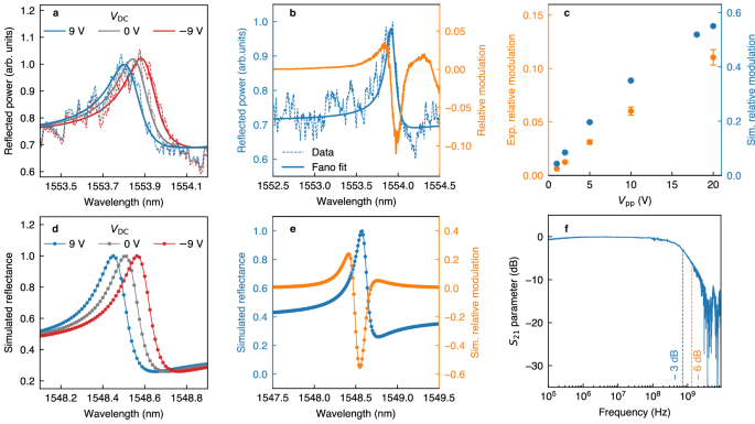
a Resonance shift upon driving the metasurface with a static bias VDC. The dashed lines correspond to the reflected intensity for three different values of VDC, the solid lines are obtained by fitting the data with a Fano profile. b Relative modulation (in orange), defined as the ratio \({P}_{\omega }(f={f}_{{\mathrm{mod}}})/{P}_{\omega }(f=0)\), where \({P}_{\omega }(f={f}_{{\mathrm{mod}}})\) is the signal demodulated at the modulation frequency fmod and \({P}_{\omega }(f=0)\) is the DC component of the signal, corresponding to the reflectance. The sinusoidal driving field is characterized by a peak-to-peak amplitude Vpp = 20 V and a frequency fmod = 100 kHz. The bias VDC is set to 0. In blue, the reflectance spectrum (dashed) and its Fano profile fit (solid). The wavelength is swept in steps of 10 pm. c Experimental (orange) and simulated (in blue) variation of the maximum modulation with respect to the peak-to-peak modulating amplitude Vpp. Experimental points are obtained by modulating with fmod = 100 kHz. d Reflectance for different applied VDC values and e reflectance spectrum and relative modulation (orange dots) simulated using COMSOL Multiphysics. The relative modulation is calculated as \([{P}_{\omega }({V=V}_{{pp}}/2)-{P}_{\omega }\left(V=0\right)]/{P}_{\omega }(V=0)\), with Vpp = 20 V. f Device frequency response obtained by calculating the parameter \({S}_{21}=10{\log }_{10}[{P}_{\omega }(f)/{P}_{\omega }^{\max }(f)]\) with a vector-network analyzer (VNA). The VNA oscillator drives the sample with Vpp = 1.5 V. All the panels refer to theoretical and experimental investigations on the sample with FF = 0.3 and α = 0.19. The optical field is polarized along the z axis (see Fig. 2).
We performed the analysis of the modulation efficiency on several fabricated designs, always obtaining values between 0.05 and 0.1 for Vpp = 10 V (see Supplementary Information S3). To complete the investigation, we studied the efficiency of the TM mode, obtaining a reduced modulation depth (see Fig. S5, Supplementary Information) caused both by the smaller electro-optic coefficient r13 = 10.3 pm/V16 and by the slightly larger resonance width of 0.5 nm (see Fig. 2h).
Finally, we assessed the modulation speed of the device. To overcome the limitation set by the lock-in amplifier bandwidth (600 MHz), we employed a vector-network analyzer (VNA) operating at frequencies up to 20 GHz and delivering a bias peak-to-peak amplitude Vpp = 1.5 V (see Fig. S1b, Supplementary Information). Figure 3f displays the resulting VNA transmission parameter, defined as \({S}_{21}=10{\log }_{10}[{P}_{\omega }(f)/{P}_{{{\rm{\omega }}}}^{\max }(f)]\), where\(\,{P}_{\omega }(f)\) is the AC component of the modulated optical signal and \({P}_{{{\rm{s}}}}^{\max }(f)\) is its maximum value in the considered frequency range. We show a –3 dB (−6 dB) attenuation for a driving frequency f−3dB \(\simeq\) 800 MHz (f−6dB \(\simeq\) 1.4 GHz). Possibly, a larger bandwidth could be obtained by reducing the length of the interdigitated electrodes, which is currently 1.5 mm, since their capacitance scales linearly with the length. The limit for the increased frequency will be imposed by a trade-off between the electrode length and the metasurface area, which needs a minimal size to sustain high Q optical resonances due to the nonlocal character of the mode.
SHG modulation
The observed modulation shown in the previous section is inherently limited by the imbalance between the high reflected power \({P}_{\omega }(V=0)\) and the effective modulated power \({\Delta P}_{\omega }(\Delta V={V}_{{{\rm{pp}}}}/2)\). This imposes a natural upper limit on the modulation amplitude, governed by the intrinsic resonance depth, which corresponds to the ratio between the maximum and the minimum values of the Fano profile over the background. For example, considering the measured reflectance spectrum shown in Fig. 3c, the maximum modulation achievable by a complete shift from the resonance peak \({P}_{\omega }^{\max }\) to off-resonance \({P}_{\omega }^{{{\rm{off}}}}\) would yield \(({P}_{\omega }^{\max }{-P}_{\omega }^{{{\rm{off}}}})\,/{P}_{\omega }^{\max }\,\simeq\) 0.3.
An advantage of modulating resonantly enhanced upconverted signals, such as SHG, is the increased sensitivity due to the quadratic dependence on the fundamental electric field, resulting in narrower linewidths. However, a significant drawback is the relatively low absolute conversion efficiency arising from the perturbative nature of the nonlinear process and the small interaction volume inherent to subwavelength devices. To generate substantial SH signals typically requires high peak intensities and, therefore, pulsed lasers. Yet, the broad bandwidths associated with pulsed sources often exceed the resonance wavelength shift ΔλEO achievable in ultrathin devices, making efficient EO modulation of upconverted signals a challenging task. As a result, very large bias voltages are typically required, which are incompatible with CMOS integration40. This limitation can only be circumvented by exploiting laser sources with linewidths significantly narrower than ΔλEO, combined with high-Q resonances. Recently, Anthur et al. demonstrated that the field enhancements associated with the narrow resonances of quasi-BIC modes in a III–V semiconductor metasurface allow to obtain sizeable SHG using continuous-wave (CW) pump sources, effectively compensating the reduced peak intensity41.
For this reason, we employed the same tuneable CW source used for the linear characterization also as pump for the SHG. We set the laser polarization along the largest component of the χ(2) tensor d33, corresponding to TE illumination. The generated nonlinear signal is then spectrally filtered and detected by means of a dispersive spectrometer equipped with a charge-coupled device (CCD) (see Fig. S1a, Supplementary Information). The spectrum of the collected signal clearly shows the SH peak (see Fig. S6, Supplementary Information) without any incoherent background. We characterize the SH signal as a function of the wavelength of the pump, with a pumping intensity of 12 kW/cm2 (see Fig. 4b).
Fig. 4: Second harmonic modulation by CD electrical stimuli.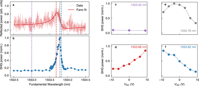
a Spectrum of the reflected signal from the sample with FF = 0.3 and α = 0.19 (see also the Supplementary Information, section S6 for the sample with FF = 0.5). b Normalized SHG excitation spectrum, obtained by sweeping the wavelength of the fundamental beam with a constant optical intensity on the sample of 12 kW/cm2. c–f EO modulation of SHG, excited with four different wavelengths (identified by vertical dashed lines in a, b depending on the applied DC voltage VDC.
The data reveal a full width at half maximum of the SHG excitation spectrum of \(\delta {\lambda }_{{{\rm{SHG}}}}\,=\,0.14\,{{\rm{nm}}}\simeq \frac{\,\delta {\lambda }_{0}^{\exp }}{\sqrt{2}}\). The SHG peak aligns with the maximum of the electromagnetic energy stored in LiNbO3, which notably does not correspond to the maximum of the reflectance spectrum shown in Fig. 4a due to the asymmetry in the Fano line shape (see Fig. S7, Supplementary Information). To tune the SHG emission via the Pockels effect, we selected various excitation wavelengths (represented by vertical, dashed lines in Fig. 4b, corresponding to the SHG peak, its inflection points, and to off-resonant excitation), while varying the applied static voltage VDC. In case of on-resonance pumping (as in Fig. 4e), we report a reduction up to a factor of 5 upon application of ΔVDC = ± 9 V. The change in intensity becomes monotonic when the excitation is tuned on the slopes of the SHG peak (Fig. 4d, f), with \([{P}_{{SHG}}\left(9{V}\right)-{P}_{{SHG}}(0{V})]/{P}_{{SHG}}(0{V}) > 1.1\) of relative SHG intensity variation by applying ΔVDC = 9 V, which is in good agreement with the nonlinear simulation under same excitation conditions (a factor 2 higher, see Fig. S8, Supplementary Information). Notably, we reach a modulation efficiency \(\eta=\,\frac{\Delta {P}_{{{\rm{SHG}}}}}{{P}_{{{\rm{SHG}}}}}/{\Delta V}_{{DC}} > 0.12\,{V}^{-1}\) The opposing trends shown in Fig. 4d, f with respect to the sign of VDC confirm the genuine electro-optic origin of the change in the SHG power (namely, VDC > 0 V leads to a blue-shift of the resonance, enhancing/suppressing the SHG when excited on the rising/falling slope of the SHG excitation spectrum, respectively). Off-resonant excitation, on the other hand, shows low SHG signal intensity and no electro-optic modulation thereof (Fig. 4c). Importantly, the low SHG signal outside the resonance leads to a high modulation efficiency, close to the simulated value. This is in striking contrast with the linear case, where the modulation is limited by a large reflectance baseline. We note that the maximum modulation that could be obtained with a complete shift of the resonance is only limited by a non-zero off-resonant SHG contribution.