Figure 1a shows one of our large-angle twisted bilayer graphene (LATBG) devices with a twist angle of \(\theta \sim 20^\circ\) (See “Methods” for the details of the device fabrication). Using gold top and graphite bottom gates we can independently set the out-of-plane displacement field D and the total charge density \({n}_{{{{\rm{tot}}}}}\).
Fig. 1: Characterization of a large-angle twisted bilayer graphene (LATBG) device.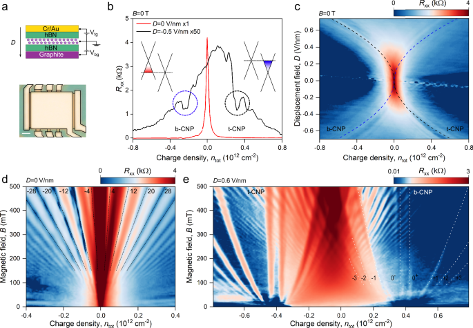
a Top panel: schematic structure of LATBG device, utilizing thin hBN flakes as dielectrics for bottom graphite and top metal gates, \({V}_{{\mbox{tg}}}\) and \({V}_{{\mbox{bg}}}\) are top and bottom gate voltages; bottom panel: optical image of LATBG Hall bar device. Black line highlights the metallic top gate and electrical contacts. Scale bar is 1 μm. b Longitudinal resistivity as a function of total charge density \({n}_{{\mbox{tot}}}\) for D = 0 V/nm, and D = 0.5 V/nm measured at zero magnetic field. Dashed circles indicate the positions of charge neutrality points of top (t-CNP, black circle) and bottom graphene layers (b-CNP, blue circle) calculated using the electrostatic model (see Supplementary Note 1). Insets schematically show band structure of LATBG under applied D when the Fermi level crosses the CNP of one of the graphene layers; here, the red part of the cone represents hole doping, and blue represents electron doping of graphene. c Longitudinal resistivity at B = 0 T as a function of \({n}_{{\mbox{tot}}}\) and D. Dashed lines indicate expected positions of CNPs. d, e Resistivity as a function of magnetic field B and \({n}_{{\mbox{tot}}}\) for D = 0 V/nm (d) and D = 0.6 V/nm (e). In (d) dashed lines show the expected position of doubled graphene filling factors. In (e) white dashed lines are a guide for the eye of the first three Landau levels and CNP gap boundaries in bottom graphene layer. See the text for the further discussion. Further examples of Landau fan measurements are shown in Supplementary Figs. 2 and 4. The high magnetoresistance observed around \({n}_{{\mbox{tot}}}=0\) can be attributed to the compensated semimetal state, similar to ref. 24, which naturally forms under applied D when one layer is electron-doped and the other is hole-doped. Measurements were performed at 2 K for all panels.
Firstly, we characterized the LATBG device by measuring its resistance at zero D, as shown in Fig. 1b. Under such conditions, both layers have the same doping, and the system behaves similarly to single-layer graphene: resistance sharply peaks at zero carrier density and rapidly drops when doping increases. Using this curve, we estimate inhomogeneity of individual layers \({{{\rm{\delta }}}}n\sim {7\times 10}^{9}{{\mbox{cm}}}^{-2}\), and electron mobility \({\mu }_{{\mbox{e}}}=0.5\times {10}^{6}\, {{\mbox{cm}}}^{2}/{{{\rm{Vs}}}}\) (Supplementary Fig. 1), which is consistent with that of a typical high-quality encapsulated devices reported in the literature9,10,11,12,13,14,15,16,17,18,19,20,21,22,23,24.
Qualitatively, the applied D creates an interlayer potential difference that separates the Dirac cones in energy, whereas \({n}_{{\mbox{tot}}}\) moves the common Fermi level (see inset Fig. 1b). When the Fermi level crosses the Dirac points, it is reflected as resistivity wiggles at positive and negative doping levels, as shown in Fig. 1b. The dual-gate map in Fig. 1c further shows how Dirac cone offset evolves upon changing D. Dashed lines mark the expected positions of Dirac points of top and bottom layers which coincide well with resistivity features that we attributed to CNPs earlier.
Screening enabled quantization in milli-Tesla magnetic field
Next, to test the device quality, we measured Landau fan diagrams under different displacement fields. When D = 0 V/nm (Fig. 1d) LATBG shows a typical Landau fan diagram of single-layer graphene, but with doubled filling factors, as expected for two graphene layers with equal doping. The applied D significantly alters this picture: in Fig. 1e, there are two sets of fan diagrams converging around \({n}_{{\mbox{tot}}}=\pm 0.4\times {10}^{12}\, {{\mbox{cm}}}^{-2}\), which correspond to the expected positions of the top and bottom graphene CNPs. These fans can be attributed to the individual quantization of the top and bottom layers, and their parabolic-like shape originates from the presence of the other heavily doped layer (see the schematic band structure in Fig. 2a and Supplementary Note 1). If plotted as a function of the charge density in top or bottom layer, the fan diagrams restore their linearity (Supplementary Fig. 2) and become similar to those shown in Fig. 1d.
Fig. 2: Resolving the onset of Landau quantization in milli-Tesla magnetic field.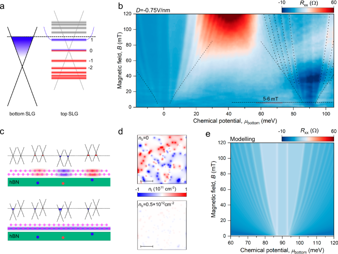
a Schematic illustration of LATBG band structure at low magnetic field B and high D when Fermi level is tuned close to the CNP of one of graphene layers. b Fan diagram measured at D = −0.75 V/nm and 2 K shown as a function of chemical potential in the bottom graphene layer \({\mu }_{{\mbox{b}}}\). Black parabolic dashed lines indicate the expected position for the first five Landau levels (LLs) plotted using a standard graphene sequence \({E}_{{\mbox{N}}}=\sqrt{2\hslash {eB}{v}_{{\mbox{F}}}^{2}N+{\varDelta }^{2}}\), where \(\hslash\) is the reduced Plank constant, \(e\) is the electron charge, \({E}_{{\mbox{N}}}\) is the energy of the \({N}^{{\mbox{th}}}\) LL, and \({v}_{{\mbox{F}}}\) is the Fermi velocity in graphene, \(2\varDelta\) is a band gap discussed further in the text. The horizontal dashed line and the error bar mark the onset of Landau quantisation. Square root dashed lines indicate the limit of quantization set by the probe width (see Supplementary Note 5). c Schematic illustrations of electron-hole puddles in LATBG at zero (top) and under applied (bottom) displacement fields. Red and blue shaded regions represent positive and negative doping correspondingly, coloured circles in the hBN illustrate charged defects. d Simulated charge density profiles in top graphene calculated for hBN with impurity density \({n}_{{\mbox{imp}}}={10}^{10}\, {{\mbox{cm}}}^{-2}\) at zero doping of the bottom layer nb = 0, and for nb = 0.5 × 1012 cm−2 (see Supplementary Note 6). Scale bars are 250 nm. e Modelling of LATBG resistance subjected to high D under the assumption of a gapped graphene spectra (see Supplementary Note 7).
An important difference between the fan diagrams observed in Fig. 1d, e is the magnetic field required to resolve the onset of Landau quantization. At D = 0 V/nm, Landau levels (LLs) become resolvable around \({B}^{*}\approx 100\,{{{\rm{mT}}}}\), while the applied displacement field significantly lowers this onset. To determine the onset of oscillations under an applied D we have zoomed into a small magnetic field range, as shown in Fig. 2b. In this map, the signatures of Landau fans become visible already at \({B}^{*}=5-6\,{{{\rm{mT}}}}\) (see Supplementary Fig. 11 and Supplementary Note 5), which is an order of magnitude better than the magnetic field required to see the Landau quantisation at zero D in LATBG and in test graphene devices without proximity screening (Supplementary Fig. 8).
A reduction of magnetic field required to resolve the onset of quantization in Figs. 1e and 2b indicates a decrease of charge inhomogeneity \({{{\rm{\delta }}}}n\) under applied D. Qualitatively, to resolve the first cyclotron gap in graphene, the fluctuations of the Fermi level must be smaller than the size of the first cyclotron gap30. To crosscheck this criterion, we modelled DoS of graphene for given inhomogeneity level, magnetic field and temperature as a function of Fermi level and energy fluctuations \({{{\rm{\delta }}}}E\) (see Supplementary Fig. 9 and Supplementary Note 4). When D = 0 V/nm and \({B}^{*}=100\,{{{\rm{mT}}}}\) (\({B}^{*}\) is the smallest magnetic field allowing resolution of the first LL), the model suggests \({{{\rm{\delta }}}}n\approx {5\times 10}^{9}{{\mbox{cm}}}^{-2}\), which agrees with earlier estimations. Under applied D (for \({B}^{*}=5-6\,{{{\rm{mT}}}}\)) we find that inhomogeneity drops to \({{{\rm{\delta }}}}n\approx 2-3\times {10}^{8}\, {{\mbox{cm}}}^{-2}\), corresponding to just 2–3 electrons per micrometre area of the Hall bar shown in Fig. 1a. However, at small magnetic fields, the cyclotron radius Rc becomes comparable to the width of our voltage probes W, which possibly limits the resolution of quantization onset. To show this, in Fig. 2c, we plotted the W = 2Rc condition, which well describes the onset of Landau quantization in our device, indicating that the quality of the LATBG device likely to be even better than estimated above. Finally, while quantization becomes apparent already at 5–6 mT, we estimate that the quantum Hall effect fully onsets at 13 mT (see Supplementary Note 5). However, at low B, zero resistivity within the cyclotron gaps is not observed because of parallel conduction through the second strongly doped layer, which remains non-quantized and contributes a significant background signal.
The suppression of \({{{\rm{\delta }}}}n\) under applied displacement field originates from the tuneable screening, in agreement with the design of our experiment. The screening of an external electric field by metallic layers is set by the DoS around the Fermi energy, which drops to zero when both layers are simultaneously tuned towards CNP (D = 0 case). As a result, any charged impurities within the encapsulating hBN crystals create substantial spatial fluctuations in carrier density, as illustrated in the top panel of Fig. 2c. On the contrary, the applied D creates an energy offset between Dirac cones of different layers which entails that the double layer device has high DoS even when one of graphene layers is tuned towards the CNP. It results in screening of external electric field and improves the homogeneity of graphene layers, as shown in bottom panel of Fig. 2c. This behavior can be quantitatively described using the Thomas–Fermi model (see Supplementary Note 6) and 2D maps in Fig. 2d, which show how the screening layer suppresses charge inhomogeneity. We also note that the analysis above primarily focuses on the energy gap between the 0th and 1st Landau levels. This gap is the largest and, due to the low intrinsic doping of graphene at this filling, is expected to be the most sensitive to external screening. In contrast, higher Landau level gaps typically emerge only at larger carrier densities, where enhanced self-screening within the quantized graphene layer reduces its susceptibility to external screening.
Resolving the gap at the CNP of graphene layers
Another notable difference between the measurements at zero and the applied D is the presence of two magnetic field-independent resistance peaks in the centres of the fan diagrams of each graphene layer in Figs. 1e and 2b. To understand these features, we perform spectroscopy of the top layer by plotting its fan diagram as a function of chemical potential in the bottom layer \({\mu }_{{\mbox{b}}}\), see Fig. 2b. The theoretical positions of the first few LLs, indicated by dashed lines, align well with the resistivity features on this map, except that instead of a single vertical resistivity peak expected for zero-energy LL, there are two peaks. This suggests the formation of a gap at the CNPs, estimated to be \({\Delta }_{{\mbox{g}}}=5\pm 1\) meV in both layers. Furthermore, we found that the gap is present even at zero magnetic field, as shown in high-resolution fan diagram, magnetic focusing measurements, and bulk-current fan diagram (Supplementary Figs. 2 and 4). It is independent of D and becomes resolvable already at D = 0.05 V/nm (see Supplementary Figs. 3 and 5).
To verify the presence of the band gap, we modelled the fan diagram of a double layer graphene system, assuming a gap at the CNP of the quantized layer. Usually, such a gap should produce a local resistance maximum, which is not observed in our devices. To reproduce the measurements shown in Fig. 2b, we had to additionally assume valley decoupling in the gapped graphene layer, as discussed in Supplementary Note 7, which leads to the edge conductivity channels inside the gap. The results of our modelling, Fig. 2e, capture the measurements shown in Fig. 2b, confirming that the two vertical resistance peaks originate from the gap edges, with their separation set by the gap size. The possible origin of this gap is discussed further in the text.
Graphene fully encapsulated with screening graphene layers
Apart from LATBG devices, where graphene serves as a substrate for another graphene layer, we fabricated large-angle twisted trilayer graphene (LATTG) devices to showcase full encapsulation of the middle graphene layer. Optical images of fabricated devices are shown in Fig. 3a. See “Methods” for fabrication details.
Fig. 3: High quality of LATTG devices.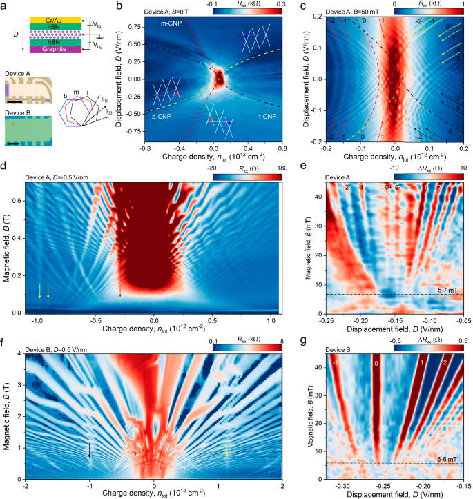
a Schematic structure of LATTG devices, graphene layers (b, m, and t labels indicate bottom, middle, and top layers, respectively) are twisted by large angles \({\theta }_{12}\) (the angle between the bottom and the middle layers) and \({\theta }_{23}\) (the angle between the middle and the top layers). See “Methods” for further information. Optical images show two measured LATTG Hall bar devices A and B, scale bar is 5 μm. b Longitudinal resistance at B = 0 T as a function of charge density \({n}_{{\mbox{tot}}}\) and displacement field D measured in device A. Coloured lines indicate conditions of CNP for top, middle, and bottom layers with black, red, and yellow correspondingly. Inset band structures illustrate the position of CNPs of each layer. c Longitudinal resistance at B = 50 mT as a function of \({n}_{{\mbox{tot}}}\) and D measured in device A. Coloured dashed lines show the calculated CNP positions for all three layers based on the electrostatic model described in the Supplementary Note 1. We therefore label the nearest Landau levels as ±1, ±2, with the sign reflecting the charge carrier type in each layer. d–g Magnetoresistance measurements for devices A and B. d, f Measured for fixed D = −0.5 V/nm and D = 0.5 V/nm correspondingly as a function of \({n}_{{\mbox{tot}}}\), coloured arrows show positions of CNPs. e, g Longitudinal resistance measured for fixed \({n}_{{\mbox{tot}}}\) as a function of D with removed background (see Supplementary Fig. 10 for more details). Onset of Landau quantisation become resolvable already at \({B}^{*}=5-7\) mT in (e) and at \({B}^{*}=5-6\) mT in (g). Measurements were done at 2 K for all panels.
To characterize LATTG, we firstly measured resistance as a function of D and ntot, as shown in Fig. 3b. Similar to bilayer devices, the resistance map reveals features that evolve under an applied displacement field. Using an extended electrostatic model (see Supplementary Note 1), we identified these features as the CNPs of the individual graphene layers, indicated by dashed lines in Fig. 3b. While symmetry considerations suggest that the middle-layer CNP (m-CNP) should remain independent of D, the m-CNP in Fig. 3b shifts towards negative doping with increasing D. This behavior is reproducible across all our devices and can be explained by small energy offsets of outer graphene layers interfacing hBN39.
Next, we measured the same D vs. ntot map at a small magnetic field of B = 50 mT, as shown in Fig. 3c. At this field, all three layers become quantized and produce three sets of parallel resistivity lines (labeled by corresponding LL number). There are single resistivity peaks corresponding to zeroth LLs in top and middle layer, while in the bottom layer, the peak doubles (labeled as 0+ and 0−). This feature, similarly to observations in LATBG, corresponds to the formation of a gap. However, in this LATTG device, the gap is resolved only in one of the layers.
To further assess the quality of our LATTG devices, we measured fan diagrams under fixed D or \({n}_{{\mbox{tot}}}\), shown in Fig. 3d–g and Supplementary Fig. 22. In all LATTG devices, we observed three sets of Landau fans converging at carrier densities corresponding to the expected positions of the CNPs for individual layers, as indicated by the arrows in Fig. 3d and f. Notably, in Fig. 3f, the complete lifting of the zeroth Landau level degeneracy is resolvable at magnetic fields as low as 1 Tesla, while it is not seen in devices without screening at similar field ranges. The high-resolution fan diagrams at small magnetic fields shown in Fig. 3e and g reveal the onset of Landau quantization already at 5–7 mT (see Supplementary Note 5 and Supplementary Fig. 12) for two different LATTG devices, showcasing the high electronic quality of graphene in such structures.