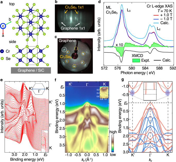
Fabrication and characterization of ML Cr2Se3
First, we present fabrication and characterization of a ML Cr2Se3 film. Since Cr chalcogenides are stabilized with a few different chemical compositions such as CrSe2 (12 phase)38,39 and Cr2Se3 (23 phase)26, it is important to identify the 23-phase nature of our film. The reflection high-energy electron diffraction (RHEED) pattern of the fabricated film shows clear streaks associated with the 1 × 1 structure of Cr2Se3, besides the 1 × 1 pattern from 2 ML graphene (Fig. 1b). The estimated in-plane lattice constant (3.6 Å) is close to the value (3.62 Å) from the first-principles calculations31 and supports the formation of the 23 phase, as directly confirmed by the transmission electron microscopy (TEM) measurements (for details, see Figs. S1–S3 in Supplementary Note 1). Low-energy electron diffraction (LEED) pattern shows sharp six-fold 1 × 1 spots originating from the Cr2Se3 film besides the 1 × 1 spots of graphene (Fig. 1c), indicative of its high single crystallinity. The clear observation of graphene spots in RHEED and LEED patterns is a signature of ML formation, as reported in TMDs40,41,42. Soft X-ray (SX) photoemission spectroscopy shows Cr3+ features and supports the formation of the 23 phase (for details, see Fig. S4 of Supplementary Note 2). To clarify possible ferromagnetism, we carried out x-ray absorption spectroscopy (XAS) and magnetic circular dichroism (XMCD) at the Cr L edge (2p-3d transition). The XAS spectrum at T = 70 K for both positive and negative out-of-plane magnetic field (\(\pm \,\)1.0 T) shown in Fig. 1d is characterized by the Cr L3 and L2 main peaks at hν ~ 577 eV and 585 eV, respectively. The XAS spectra show a small but finite difference between the +1.0 T and −1.0 T, signifying a finite XMCD signal indicative of ferromagnetism. This is better visualized by the difference spectrum plotted on an expanded y-scale (green area) in which the overall XMCD spectral shape is consistent with that of ML Cr2Se3 and Cr2Te330,43,44. Cluster model calculations are consistent with experiments (Fig. 1d) and indicate that ML Cr2Se3 is a negative-charge transfer material with Cr3+ t2g3↑ configuration and a magnetic moment of 3.4 μB/Cr-atom (for details, see Supplementary Note 3). These results suggest that the 2D magnetism is realized in a non-van der Waals material. Since non-van der Waals 2D materials in the ultrathin limit cannot be easily obtained by a simple mechanical exfoliation of bulk crystal, the present result indicates the importance of molecular-beam epitaxy (MBE) for realizing properties unique to non-van der Waals 2D epitaxial films. One also expects a stronger interfacial effect with other materials due to the absence of a van der Waals gap, which would be useful for modulating or enhancing the magnetic properties.
To clarify the electronic states relevant to the occurrence of ferromagnetism, we investigated the band structure in the FM phase. Energy distribution curves (EDCs) measured along the ΓK cut of the hexagonal Brillouin zone (inset) in Fig. 1e signify highly dispersive valence bands located at the binding energy (EB) of 1–3 eV, whereas the intensity within the EB range of 0–1 eV is suppressed due to the band-gap opening. A careful look in close vicinity of EF around the K point reveals the existence of a Fermi-edge cut-off indicative of the metallic nature. This is due to the appearance of an electron pocket as seen in the magnified EDCs and corresponding intensity plots (insets of Fig. 1e, f). The overall valence-band structure is better visualized by the ARPES-intensity plot as a function of ky and EB in Fig. 1f which displays the complex band structure characterized by several holelike bands centered at the Γ point and an M-shaped band around EB ~ 2–2.5 eV. From the energy separation between the top of valence bands at the Γ point and the bottom of conduction bands at the K point, it is suggested that ML Cr2Se3 is a semiconductor in non-doped regime with an indirect band gap of ~0.8 eV. As shown by a side-by-side comparison of Fig. 1f, g, the overall band structure determined by ARPES shows a qualitative agreement with the calculated band structure for free-standing ML Cr2Se3 obtained from first-principles calculations for the FM phase assuming out-of-plane magnetic moments and an on-site Coulomb energy of U = 3.5 eV31. For example, the experimental holelike band topped at the Γ point shows a good correspondence to the top of calculated up-spin bands (red curves), and the M-shaped down-spin bands (blue curves) are commonly recognized at ~1 eV below the valence-band top, in both the experiment and calculation. The momentum location (the K point) of the bottom of the conduction band which is assigned to the up-spin Cr 3d eg↑ band is also well reproduced by the calculation although the calculation underestimates the band-gap magnitude by ~30%. The appearance of the eg↑ electron pocket suggests that ML Cr2Se3 grown on 2 ML graphene is a doped semiconductor with half-metallic nature. To identify the orbital character of observed bands, we carried out resonant ARPES measurements using SX photons around the Cr L3 absorption edge (for details, see Fig. S5 of Supplementary Note 4). The results show a strong resonance enhancement of ARPES intensities at EB ~ 1.5–2.5 eV associated with the Cr 3d-t2g↑ bands hybridized with the Se 4p states (for details of the orbital assignments, see Supplementary Note 5).
Temperature dependence of the band structure across T
C
Now that the overall band structure in the FM phase is established, next we show temperature evolution of the band structure in Fig. 2a–c (detailed T-dependence is shown in Fig. S13). Key characteristics of the complex band structure seen at T = 40 K in Figs. 1f, 2a, such as the M-shaped band around EB ~ 2–2.5 eV and a sharp valence-band top at the Γ point, still persist at T = 150 K (Fig. 2b). In contrast, at T = 300 K (Fig. 2c), the spectral feature becomes simpler and the M-shaped band is converted to a V-shaped band located around EB ~ 1.3–2.1 eV. As shown later, the detailed analysis and temperature-dependent XMCD measurements suggest that TC lies between 225 and 250 K, higher than the estimated TC value of ~200 K in ML Cr2Se3 on HOPG30.
Fig. 2: Temperature evolution of band structure and evidence for spin-valley polarization.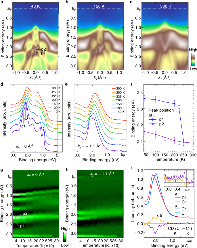
a–c ARPES-intensity plots along the ΓK cut measured at T = 40 K, 150 K, and 300 K, respectively, measured with circularly polarized photons of hν = 75 eV. Peaks p1 and p2 are also indicated. d, e Temperature-dependence of EDCs at selected k cuts at ky = 0.0 (Γ), −1.1 Å−1 (K’), respectively. f Temperature dependence of the peak position for valence-band peaks at EB ~ 2–2.5 eV at the Γ point (ky = 0 Å−1) estimated by numerical fittings to the EDCs assuming Voigt peaks and linear background with error bars ± 20 meV. g, h Second-derivative intensity plots of Fig. 2d, e, respectively. i EDCs for ML Cr2Se3, obtained at the K and K’ points with C+ and C- polarized lights using hν = 75 eV. Yellow and purple curves represent subtracted EDCs obtained with C+ and C- photons expanded vertically by 5 times. Inset shows the expansion near EF. One can recognize a clear circular dichroism (CD) associated with spin-valley polarization which reverses its sign between the K and K’ points.
Besides a drastic change in the band structure, a systematic T-dependent energy shift is observed in the EDCs and corresponding second-derivative intensity plots at the Γ point (ky = 0.0 Å−1) in Fig. 2d, g. All the bands, including the topmost valence band and corresponding spin-orbit split Se 4p states separated by ~0.2 eV45, systematically move toward EF on increasing temperature upto TC, with a gradual increase in the peak width associated with thermal broadening. This is also the case for the spectra at the K’ point (ky = − 1.1 Å-1; Fig. 2e, h). Besides the systematic band shift, some bands show additional energy splitting at low temperatures. For example, at the Γ point (Fig. 2d), a main peak at EB = 2.16 eV with a shoulder feature at 2.36 eV at T = 40 K, signify the existence of a double peak (marked as p1 and p2 in Fig. 2d). This double peak consisting of Cr-Se hybridized states constituting the M-shaped band get merged into a single peak on increasing temperature, around T = 225–250 K. We quantified the T-dependence of band energies from numerical fits to the EDCs and the peak positions are shown in Fig. 2f. The band splitting vanishes between T = 225–250 K, corresponding to TC of ML Cr2Se3. The same trend is also recognized for the peaks at ~1.97 eV and ~2.13 eV at T = 40 K for the K’ point (Fig. 2e, h) and corresponding plots of the t2g band energies in Fig. S7c (for details, see Supplementary Note 6). We attribute the above observation to the band splitting associated with the FM transition, since the splitting sets in around TC, as is also confirmed by the T-dependent XMCD signal shown in Fig. S18. Such a clear T-dependent band splitting below TC has been rarely reported in 2D ferromagnets24,46.
Spin-valley coupling
We found a signature of circular dichroism (CD) for the t2g↑ bands at the K and K’ points at T = 40 K for ML Cr2Se3, as shown Fig. 2i. Using right and left circularly polarized light (C+ and C-), the obtained EDCs at the K point (red and pink curves) show a difference between their peak intensities, signifying a finite CD. This CD is also observed at the K’ point (blue and light blue curves) but with a sign reversal compared to the K point, as shown by the subtracted EDCs expanded vertically (yellow and purple curves). We found a sign reversal of CD also for the eg↑ pocket between the K and K’ points (see inset to Fig. 2i). Intriguingly, the sign is also reversed between the t2g↑ and eg↑ bands. These observations suggest that photoelectron excitations are asymmetric between the K and K’ points, supporting the valley-selective CD (i.e., valley polarization) which is a necessary condition for realizing anomalous valley Hall effect31. It is noted that the observed CD is not likely to originate from experimental artifacts such as incomplete CD polarization or sample degradation, but is an intrinsic property of our Cr2Se3 film (for details, see Supplementary Note 7). This is also corroborated by the observation of three-fold symmetric LEED pattern suggestive of the inequivalently mixed structure domains rotated by 60° from each other (in this regard, it is different from ML 1 T’ TMDs with equivalently mixed 120° rotated domains47,48,49,50), making our Cr2Se3 film a valid candidate to observe valley polarization (for details, see Fig. S8 and Supplementary Note 7).
We found that the overall magnitude of CD is reduced in the 2 ML sample with lower TC (see Fig. S9 in Supplementary Note 7), signifying that the valley-selective CD is coupled to the ferromagnetism. This coupling of localized t2g-spins and itinerant eg-valley states is supported by considering the magnitude of experimental energy splitting for the strongly hybridized t2g bands at the K/K’ point for ML (~160 meV) which is much larger than the SOC energy (ΔSOC) of Cr3+ states (~50 meV) and inversion-symmetry breaking of the crystal (at most a few tens meV)31. But the observed splitting is comparable to the known ΔSOC of ~200 meV in Se bands45, which is about half of the atomic SOC energy Δ’SOC = 418 meV for Se 4p states. In a recent study on V1/3NbS2 crystals, a giant valley-Zeeman coupling in surface states of the NbS2-termination top layer was reported to originate from hybridized V d orbitals and planar NbS2 orbitals with an exchange splitting Δex ~ 52 meV and ΔSOC ~ 59 meV aiding each other at the K point and opposing each other at the K’ point. Using known values of valley-Zeeman splitting of ~0.2 meVT−1 for TMDs51, the authors estimated that a magnetic field exceeding 250 T was operative in V1/3NbS2 to give the observed splitting. However, the results showed that the surface states of V1/3NbS2 exhibit the same magnetic ordering temperature as the bulk, with TN ~ 53 K37. In the present case, we see ferromagnetism with a relatively high TC ~ 225 K for ML Cr2Se3 case compared to an antiferromagnetic TN ~ 45 K for bulk Cr2Se326. However, we see an experimental energy splitting for the t2g bands at the K/K’ point for ML (~160 meV) suggesting a spin-splitting-dominated spin-valley coupling since the valley splitting is calculated to be just 18 meV31. Moreover, the gradual reduction of the splitting energy with a small reduction in TC by increasing number of layers (see Fig. S7 in Supplementary Note 6) also supports the intimate coupling of spin and valley degrees of freedom for an enhanced TC in 2 ML and 3 ML films compared to bulk TN ~ 45 K.
Besides the spin-valley coupling, another intriguing characteristic of ML Cr2Se3 is the evolution of the eg↑ electron pocket at the K/K’ point. The EDCs in Fig. 3a signify a sharp peak associated with the eg↑ band at T = 40 K for both the K and K’ points. Upon increasing temperature, the spectral weight of eg↑-peak is monotonically reduced and the peak has almost vanished at T = 300 K. This suggests that ferromagnetism in ML Cr2Se3 is associated with spectral weight of the eg↑ pocket. Figure 3a shows that the total spectral weight at fixed temperature is higher at the K point than at the K’ point (see purple or blue curves). This intensity asymmetry is attributed to the inequivalent valley states at the K and K’ points predicted by the density-functional-theory (DFT) calculation31 and associated with the spin-valley coupling. We have carefully examined this inequivalent valley states between the K and K’ points, and found that the asymmetric nature is reproducible for different samples. More intriguingly, the asymmetry gets enhanced after applying out-of-plane magnetic field, supporting the spin-valley coupling (for details, see Figs. S10 and S11 in Supplementary Note 8).
Fig. 3: Thickness dependence of electronic states.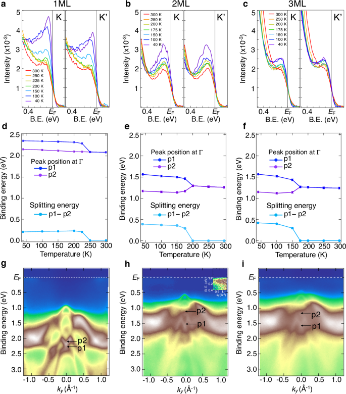
a–c Temperature dependence of EDCs near EF at the K (ky = 1.1 Å−1; left panel) and K’ (ky= −1.1 Å−1; right panel) points to the evolution of the eg↑ electron pocket for ML Cr2Se3. The spectral weight is normalized to the valence-band t2g peak. d–f Temperature dependence of the peak position for valence-band peaks p1 and p2 at the Γ point estimated by numerical fittings to the EDCs for ML, 2 ML, and 3 ML Cr2Se3, respectively, suggesting the gradual reduction of TC upon increasing the number of layers n. g–i ARPES-intensity plots as a function of ky and EB along the ΓK cut measured with hν = 75 eV photons at T = 40 K for ML, 2 ML, and 3 ML Cr2Se3, respectively. Inset to (h) shows the ARPES intensity with enhanced color contrast around the K point. B. E. stands for binding energy.
In particular, ARPES measurements on ML Cr2Se3 film with improved statistics were carried out to confirm the inequivalence of valley states at K and K’ points. ARPES intensity maps around the K’ and K points, obtained after normalizing the total spectral weight over the plotted EB range of EF to 2.7 eV (Fig. S10a, b) indicate that the intensity of the electron pocket around the K point is higher than that around the K’ point, confirming the inequivalent valley states around K and K’. Overlapped EDCs at positive ky’s and negative ky’s (Fig. S10c) clearly indicate that the spectral weight of the eg -derived peak for positive ky’s is higher than that for negative ky’s.
To clarify the possible coupling of inequivalent valley states to the spin degrees of freedom, we performed ARPES measurements after magnetizing the sample by applying an out-of-plane magnetic field with the strength of B = + 0.1 T (see EDCs in Fig. S10d). While the overall spectral intensity of the electron pocket is slightly reduced, the asymmetric intensity of the EDCs between the K and K’ points indicate that the inequivalence is preserved even after applying B. To our surprise, we found that a broad shoulder feature appears at EB ~ 0.2 eV more prominently for negative ky’s, i.e., around the K’ point, suggesting that the shape of the EDCs becomes more inequivalent after applying B. This change is highlighted by a direct comparison of EDCs at the K and K’ points (Fig. S11a, b) indicating that the spectral weight of the shoulder feature is enhanced at the K’ point after applying B, which is also confirmed by our numerical analysis of EDCs (Fig. S12). We found that the shoulder feature becomes much weaker and the EDC shows a simpler peak shape at the K’ point upon reversing B, becoming similar to the spectrum at the K point obtained by applying positive B (Fig. S11c). In addition, we confirmed that this result is reproducible for different samples, by measuring another ML Cr2Se3 sample (Fig. S11d). This finding strengthens our argument on the observation of inequivalent valley states between the K and K’ points and their coupling to the spontaneous ferromagnetism.
Band structure of multilayer Cr2Se3
Next, we fabricated 2 ML and 3 ML Cr2Se3 films to investigate thickness evolution of their band structure and relation with spin-valley states. We found that the energy bands of 2 ML and 3 ML films (Fig. 3h, i) are shifted upward by ~0.4 and ~0.5 eV, respectively, compared to the ML film (Fig. 3g). Simultaneously, the Cr 3d t2g bands get significantly broadened, and also show larger band splitting at the Γ point. Detailed analysis at the Γ point (and the K point; see Fig. S7 in Supplementary Note 6) shown in Fig. 3d–f suggests that the TC gradually decreases on increasing the number of layers n; TC = 225–250 K, 175–200 K, and 150–175 K, for ML, 2 ML, and 3 ML, respectively (for detailed T-dependent ARPES data and quantitative analyses of the band splitting, see Figs. S13–17 in Supplementary Note 9). We have confirmed that TC’s estimated by ARPES and XMCD well coincide with each other, suggesting the validity of the TC estimation from the band splitting (for details, see Fig. S18 in Supplementary Note 10). The TC reduction is correlated with the spectral weight at EF of metallic eg↑ pocket seen for ML (Fig. 3a), which gets reduced in 2 ML (Fig. 3b) and almost vanishes in 3 ML (Fig. 3c) (note that a tiny electron pocket still exists at low temperatures for 2 ML, as seen in the image with enhanced color contrast in the inset to Fig. 3h). This is consistent with the observed valence-band shifts on increasing n and indicates that the highest doping of electron carriers occurs in the ML film at low-T. It is noted that the asymmetric intensity distribution of the eg↑ band between the K and K’ points observed for ML gets reduced for 2 ML and 3 ML (Fig. 3b, c), confirming the coupling of valley anisotropy and ferromagnetism. Interestingly, a very recent study24 on Cr2Te3 showed that 3 ML and 6 ML films with TC = 170 K and T-dependent band shifts, exhibit a reduced TC = 90 K in ML with no energy band shifts, indicating a Stoner to Heisenberg (itinerant to localized)-type FM order. In contrast, Cr2Se3 shows an enhancement of TC in the ML case with TC ~ 225 K compared to 2 ML (TC ~ 175 K) and 3 ML films (TC ~ 150 K), derived from spin-valley coupling of localized and itinerant states.
The most reasonable explanation of the observed n-dependent band structure and FM TC’s is the charge transfer from the graphene substrate39,52, which is also supported by directly comparing the binding energy of the Dirac point of graphene bands before and after the fabrication of ML Cr2Se3 (for details, see Fig. S19 in Supplementary Note 11). Accordingly, the doped electron carrier density per unit Cr2Se3 layer is expected to be reduced for multilayer films since the total amount of transferred charge carriers across the interface is fixed; this behavior is realized in the present study. Since the Mermin-Wagner theorem12 suggests that FM order is suppressed upon reducing n, in contrast to present observations, the enhancement of TC up to 225–250 K in ML is likely due to the RKKY mechanism associated with maximum carrier density in eg↑ valley states. This argument also explains why the insulating ML Cr2Se3 films fabricated on Al2O3 or SiO2/Si do not show FM but AF order, as in the bulk crystal26,28,29, because no charge transfer is expected from insulating Al2O3 or SiO2/Si in contrast to the present study which uses a metallic 2 ML graphene/SiC substrate. It also explains the observation of high-TC ferromagnetism (TC ~ 200 K) for ML Cr2Se3 on HOPG30, comparable to the present work because charge-transfer characteristics of graphene and HOPG are expected to be similar with nearly equal work functions.
Finally, we discuss important differences between Cr2Se3 and Cr-Te based van der Waals ferromagnets Cr2Ge2Te6 and CrTe2. A critical difference is that tellurium compounds commonly show ferromagnetism in the bulk whereas bulk Cr2Se3 is an antiferromagnetic (TN ~ 45 K) semiconductor. Moreover, only Cr2Se3 transforms into a ferromagnetic metal with TC ~ 225 K for ML films grown on graphene (TC ~ 200 K for ML Cr2Se3/HOPG; ref. 30). In contrast, the van der Waals ferromagnets, namely Cr2Ge2Te6 (ref. 13) and CrTe2 show a reduction in TC on decreasing thickness (although there are conflicting reports for Cr2Te3 as discussed above23,24). Reference 24 showed that the dominantly Te character orbitals cross EF in Cr2Te3 and form the Fermi surface, leading to an itinerant Stoner type ferromagnetism in thick Cr2Te3 films, but for ML Cr2Te3 film, the Stoner condition is not satisfied and a local moment Heisenberg exchange driven ferromagnetism is realized. In contrast, the Se bands in Cr2Se3 sink well below EF and the occupation of the valley electron pockets with Cr 3d eg character, which couple with localized t2g spins, promotes the ferromagnetism. These aspects suggest that the origin of ferromagnetism in Cr2Se3 films on graphene or HOPG can be expected to be qualitatively different from the van der Waals ferromagnets (it is noted here that, in the ML limit, Cr2Te3 suffers from a trigonal distortion24 with a 2 × 2 superstructure whereas Cr2Se3 maintains its 1 × 1 structure, which can lead to differences in their magnetic properties). Also, the double exchange mechanism is usually considered for the case of mixed valent materials, which is unlikely for Cr2Se3 films on graphene, distinct from the situation of Cr2Ge2Te6 (refs. 53,54); for a detailed discussion, see Supplementary Note 12. Our results in Fig. 3, corroborated by temperature-dependent XMCD, suggest that the reduction of TC on increasing the number of layers is caused by a reduction in the electron carrier density transferred from the substrate across the interface. The results taken together indicate that the TC is proportional to the carrier density (this is supported by the plot of TC vs spectral density of states at EF in Fig. S20), and hence suggest that the ferromagnetism is likely due to the localized t2g spins coupled by the RKKY interaction active in the valley electron pockets of Cr2Se3 films grown on graphene.