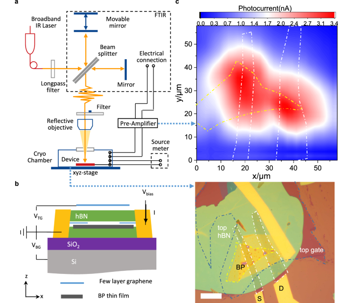
We first examine the photocurrent spectra with different layer numbers and pumping power. Experimentally, an incident broad-band laser is modulated and aligned with the sample. With a moderate source-drain bias (Vbias = 0.8 V), photo-currents both generate at the contacts by a photovoltaic-like mechanism20 and inside the channel by a photo-conductive effect. The laser is thus parked around the grounded source-electrode to maximize the photo-response by the Schottky junction and minimize any bias-dependent doping effect. It is worth noting that the spectra are nearly unchanged when slightly change doping or pumping at different positions.
Figure 2a shows the photocurrent spectra of BP with different thicknesses at low photo pumping. All the spectra present a single excitonic peak (marked by red triangles) and agree well with previous report21. The spectra obviously change with increasing pumping power, because pumping significantly modifies the photo-excited electron-hole pair density and corresponding Coulomb screening in BP. Figure 2b summarizes the pumping-dependent photo-current spectra for a 11-layer sample. As the power increases, the exciton peak (around 3400 cm−1 as indicated by the dashed brown arrows) gradually disappears. In contrast, a continuous absorption band above 3200 cm−1 emerges. The cut-off energy of this continuous absorption that features BP’s band-edge also gradually blue-shifts with increasing pumping power. We attribute these observations to Pauli-blockade effect and increased Coulomb screening at high electron-hole pair densities (Fig. 2c). Interestingly, another low energy peak rises at high pumping (around 3100 cm−1 as indicated dashed blue arrows). This signal likely originates from spatially indirect excitation between different interfaces. That is, electrons and holes tend to accumulate at bottom and top surfaces of BP, although the whole sample is still charge neutral. And the spatially separated electrons and holes form a new kind of exciton. Because vertical electric field generally drives the aforementioned charge accumulation, this spatially indirect excitation is D dependent. And its excitation photon energy is lower compared to bulk excitons, as schematically depicted in Fig. 2d. Actually, this spatially indirect excitation peak is always pronounced when applying large displacement field (Supplementary Fig. 10); but it is only visible for a few zero-gated thick samples, probably arouse from asymmetric substrate effect22,23. The corresponding photo-current should also flow through interfacial channels. It is different from the continuous absorption counterpart, which employs an intrinsic BP channel.
Fig. 2: Fourier transform infrared photocurrent spectra of BP.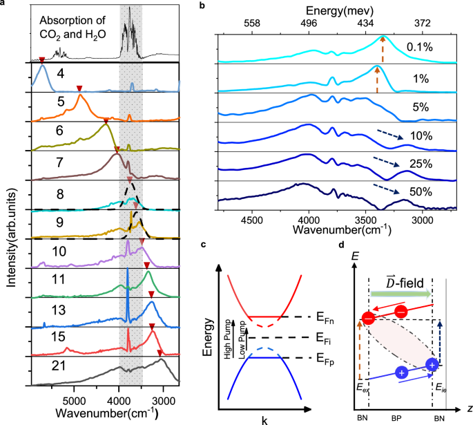
a Typical photocurrent spectra of BP with different number of layer (in arbitrary units). Photo-pumping power P = 0.13 W/cm2 and temperature T = 5 K. The top panel shows environmental background obtained by Fourier transform infrared spectroscopy. The shadow region represents the interference from moisture. The curves are shifted by multiples of two for clarity. Each exciton peak is marked by red triangle. b Photocurrent spectra of an 11-layer sample at different photo-pumping power. 100%P = 1300 W/cm2. c Schematic band dispersion of BP. The dashed and solid lines show the intrinsic and highly pumped band structure. d Schematic energy diagram of spatially indirect exciton. Under an out-of-plane displacement field, electrons and holes accumulate at the two dielectric interfaces. The spatially indirect excitation energy of Eie is lower than the intrinsic exciton energy of Eex. Dashed brown and dashed blue arrows corresponds to the peaks marked in (b).
Electrical-field tunable phase transition
Our major finding is that for BP with appropriate thickness (8–10 layers, see Supplementary Table 1 for a detailed device summary), a metal-to-insulator transition occurs at moderate displacement field and photo-pumping. We begin with a characterization of displacement field tunable bandgap in BP samples. Figure 3a shows the conductance of a 10-layer sample measured by sweeping the back gate bias at different static top gate biases. The minimum conductance (where the top gate and bottom gate doping compensate each other and are also recognized as charge neural points) at large external displacement field (D ~ 0.5 V/nm) increases about 4 orders compared to that without any field. The significant variation indicates a reduction of BP’s bandgap24,25. In fact, we can quantitatively estimate the bandgap from the minimum conductivity variation in the transport data. Briefly, the intrinsic carrier density (i.e. the carrier density at the minimum conductivity) is proportional to exp(−Eg/2kBT), where Eg is the bandgap, kB is the Boltzmann constant and T is temperature. By fitting the temperature dependent minimum conductivity of I–V curves under different D, we obtained the Eg as a function of D (shown in the inset of Fig. 3a). Supplementary Fig. 11 comprehensively shows the extracted bandgap, it shrinks from ~440 meV to D. Large D accumulates interfacial charges as aforementioned. It may quantitatively influence the estimation, but the extraction qualitatively exhibits the Eg of BP vanishes with increasing D.
Fig. 3: Displacement field dependence of dual-gate BP.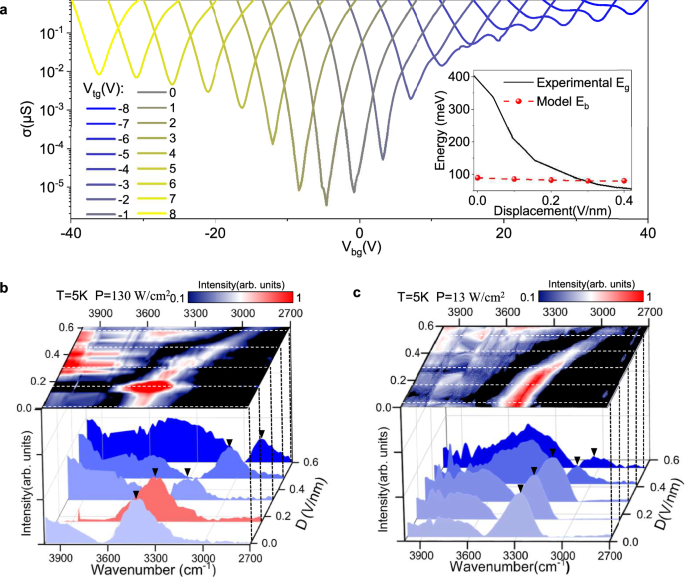
a BP conductance as a function of bottom gate voltage Vbg at different fixed top gate voltage Vtg. Inset: Measured bandgap (Eg) and calculated exciton binding energy (Eb) as a function of D. b, c Normalized photo-current spectrum of a 10-layer BP as a function of displacement field for P = 130 W/cm2 (b) and P = 13 W/cm2 (c), showing the spectral features with and without EI phase transition. The waterfall curves show the photo-current spectra at different displacement field D, selected along the white dashed lines in the top panels. The red spectrum shows EI. The black triangles mark the spatial indirect excitation peaks.
We further carry out photocurrent spectroscopy along the charge-neutral points. Figure 3b, c illustrate typical spectral evolution with increasing D for the same sample, but under different excitation intensities of 130 W/cm2 and 13 W/cm2, respectively, at 5 K. Generally, both the continuous absorption (unmarked part in Fig.3b, c) edge and the spatially indirect excitation (marked by black triangles in Fig. 3b, c) red-shift with applying displacement field. Remarkably, under 130 W/cm2 excitation and with D ranging from 0.16 to 0.22 V/nm, the spectra abruptly turn to a single-peak (the red spectrum in Fig. 3b) shape without any continuous absorption component. However, this spectral variation is absent under other conditions.
It should be noted that the sharp change from the broad-band photo-current response to the single-peak response (e.g. D = 0 to 0.2 V/nm in Fig. 3b) is due to a phase transition. We subsequently probe the gating-dependent spectra to gain a deeper understanding. Figure 4a, b plot the photo-current spectra as functions of back gate voltage at D = 0.4 and 0.19 V/nm. During the measurement, the change of top (\(\Delta {V}_{{{{\rm{t}}}}g}\)) and bottom (\(\Delta {V}_{bg}\)) gate voltages are synchronously adjusted as \(\Delta {V}_{bg}\frac{{\varepsilon }_{b}}{{d}_{b}}=\Delta {V}_{tg}\frac{{\varepsilon }_{t}}{{d}_{t}}\) to keep the vertical displacement field unchanged. For the broad-band spectra (Fig. 4a), the photo-current intensity only slightly decreases with both electron and hole (gate) doping. As the electron or hole doping level increases, the spatially indirect excitation (~3200 cm−1 as indicated by the white arrow) is replaced by a peak at lower energies (~2900 cm−1 as indicated by the dotted white arrows). It corresponds to a transition between neutral excitation and charged excitations. In stark contrast, for single-peak spectra (Fig. 4b), the photo-current is very sensitive to gating. Its magnitude rapidly decreases once (both negatively and positively) gated.
Fig. 4: Excitonic insulator and its superfluidity.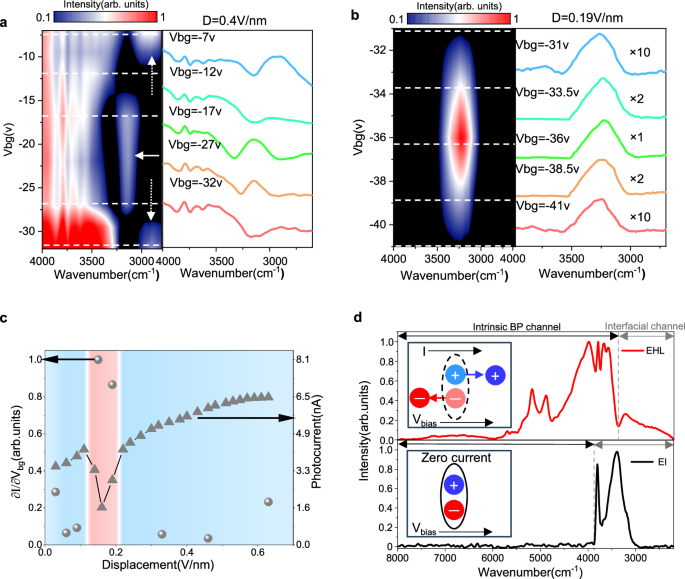
a, b Gating dependent photo-current spectra of a 10-layer BP. Right panels show the photo-current spectra at different gating, selected along the white dashed lines in left panels. Color bars represent normalized photocurrent intensity. The white arrow marks the spatially indirect excitation, and the dotted white arrows mark the charged excitations. c The partial derivative of photo-current spectra to gating (\(\partial I/\partial {V}_{g}\)) and total photocurrent as functions of D. An insulating EI phase (red region) is distinct from the non-equilibrium metallic phase (blue region). d Photo-current spectra of electron-hole liquid (EHL, upper panel for D = 0.46 V/nm) and excitonic insulator (EI, bottom panel for D = 0.17 V/nm). Insets schematically illustrate the scattering effect of Coulomb damping for normal and superfluid exciton flows.
It worth mentioning that the partial derivative of photo-current spectra to gating (\(\partial I/\partial {V}_{g}\)) around charge neutral point reflects the charge compressibility. Namely, it directly measures the carrier change in response to gate modulation and is therefore proportional to the penetration capacitance in the unit area (see Supplementary Note 1 for details). Here for better comparison, we mainly focus on the photocurrent from spatially indirect excitation (~3200 cm-1) because its transport property is relatively stable. For charge-compressible or metallic states, \(\partial I/\partial {V}_{g}\) converges to a constant value as the surface potential is almost unchanged with gating, resulting in finite charge compressibility. On the contrary, for charge-incompressible or insulating states, \(\partial I/\partial {V}_{g}\) is greatly enhanced.
To evaluate the phase transition, we summarize \(\partial I/\partial {V}_{g}\) and total photo-current as functions of D in Fig. 4c. A sudden jump of \(\partial I/\partial {V}_{g}\) coincides with the sharp spectra change (represented by photo-current reduction), suggestive of a metal-to-insulator transition. In this scenario, the broad-band absorption case is a metallic phase, whereas the single-peak case corresponds to a charge-incompressible insulating phase.
Excitonic Insulator
We argue that this insulating phase is an excitonic insulator. To verify the origin of the phase-transition, we next examine the single-particle bandgap and exciton binding energy under displacement field. Firstly, we theoretically consider the exciton binding energy as a function of D. We perform first-principle calculation to determine the quasi-particle electronic structure and excitonic state using the GW/Bethe-Salpeter Equation (BSE). Due to the computational intensity, we performed converged calculations on bilayer and four-layer BP under a vertical electric field. Based on the DFT results, we have further developed a parameter-dependent model to extend the results to eight layers whose calculation is beyond the DFT capability. We find that the binding energy of 1s exciton is not sensitive to the gate field (Fig. 3a inset also see Supplementary Note 2 for details), which challenges the traditional assumption of exciton binding energy decreases in the presence of external electric-field.
This can be interpreted as the Berry curvature altered exciton spectrum. Generally speaking, the electron-hole interaction can be described using the effective Hamiltonian in (1)26,27.
$${H}_{eff}=\frac{{\hat{p}}^{2}}{2m}+V(r)+\frac{1}{2\hslash }\Omega \cdot (\nabla V\times \hat{p})+\frac{1}{4}\Omega {\nabla }^{2}V$$
(1)
Here \(\Omega\) represents a Berry curvature of the electron-hole pair that arises when a vertical electric-field breaks the inversion symmetry of the few-layer BP. The third term is the effective spin-orbit coupling term, leading to the splitting of the p or d exciton states due to the Berry curvature27,28. In our case, \(\Omega\) aligns with the gradient of the vertical electric-field (\(\nabla V\)), resulting in no response in exciton energy splitting. And the fourth term, known as the Darwin term, increases the binding energy of the 1 s exciton with increasing electron-hole distance. It is able to compensate the reduction in binding energy due to the enhanced screening effect and enlarged electron-hole distance. Therefore, this Darwin term described Berry curvature effect is likely the main reason for the constant binding energy regardless of applied vertical electric field.
While the binding energy of interlayer exciton is almost D invariant, the bandgap gradually close with increasing D. BP has a strongly puckered lattice structure, rendering its band structure highly susceptible to a vertical D. The external field is apt to shift the real-space distribution of valence and conduction band states toward each other, which allows to tune the material from a moderate-gap semiconductor to a band-inverted semimetal24. For instance, we have experimentally demonstrated large bandgap shrinking as aforementioned. Consequently, at certain D (e.g. ~0.16 to 0.22 V/nm in the presented sample), the interlayer exciton binding energy could exceeds the closing bandgap. This picture is entirely unexpected on the basis of the single-particle band structure. It however leads to a critical point where a metal-to-exciton insulator transition happens. That is, under high photo-pumping and zero D, BP is a non-equilibrium metal whose quasi-Fermi-levels locate inside the conductance and valence bands. With increasing D, photo-injected electrons and holes pair together and form a condensate EI state as a result of the strong Coulomb correlation and closing bandgap. Further increase D or power-pumping introduces higher electron–hole density. Beyond certain threshold (estimated as about 3.4 × 1011 cm−2 from the photo-current, see Supplementary Note 3 for details), enhanced screening effect drives the insulating EI to metallic electron-hole liquids through a Mott transition.
Evidence of excitonic superfluidity
We next move to discuss the transport properties of intrinsic BP channel (marked in Fig. 4d, it corresponds to the continuous absorption part in the photo-current spectra) during the phase transition. Interestingly, all the high energy range (from band-edge to ~1 eV) photo-current drops below the noise floor accompanied with the EI formation, as highlighted in Fig. 4d. We attribute the vanishing channel photo-current as an evidence of superfluid flow of excitons. On one hand, this zero photo-current is unlikely arouse from insulating gap forbidden absorption, because it means the EI gap should be at least ~1 eV and violates temperature-dependent measurements (see below). On the other hand, the disappeared photo-current clearly indicates the collective phase of bounded electron-hole pairs in bulk BP does not dissociate (into electron/hole free carriers) at all even when exposure to external damping effect, including applied (both in-plane and out-of-plane) electric field forces. Or in other words, excitonic decay time is notably lengthened to nearly same as the lifetime of excitons. It signifies the transition of a system of excitons into a superfluid state29,30. Because in these situation, excitons do not transfer their excitation energy to environment or scattering sources, that is a superfluid by definition. Exciton flow could still be generated by diffusion or thermal driving. Through this non-dissipated motion, paired electrons and holes should arrive at the electrodes together and contribute zero net current.
We finally study the temperature dependence of EI state. It is observed that the EI phase presents a typical BCS-like temperature behavior. Figure 5a plots the photo-current spectra as functions of D, with the same photo-pumping as in Fig. 3b but at 20 K. EI states do not take place at this temperature. We define a parameter spectral weight (SW) to represent the spectral character of EI states. It equals the ratio of the spatially indirect excitation peak weight to the totally spectral weight. Thus SW approaches unity for EI state, due to the continuous absorption part vanishes. We summarize the spectral feature S.W. and \(\partial I/\partial {V}_{g}\) as functions of temperature T in Fig. 5b for a given D (0.19 V/nm). Both of SW and \(\partial I/\partial {V}_{g}\) sharply change with increasing T. It reveals EI states persist up to a critical temperature about 17 K. Overall, the temperature dependence of EI superfluidity resembles that of a super-conductor.
Fig. 5: Temperature dependence of dual-gate BP.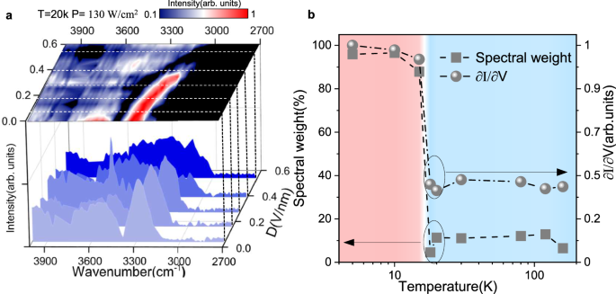
a Normalized photo-current spectrum of a 10-layer BP as a function of displacement field for T = 20 K. The waterfall curves show the photo-current spectra at different displacement field D, selected along the white dashed lines in the top panels. The color bar represents normalized photocurrent intensity. b Spectral weight of spatially indirect excitation S.W. and \(\partial I/\partial {V}_{g}\) as functions of temperature. D = 0.19 V/nm.