3D AXIs stacked from 2D
We start from the 2D single-layer QAH material hosting metallic 1D chiral edge states, depicted in Fig. 1a. Here, chirality refers to the in-plane energy flow direction respective to the out-of-plane magnetization. When reversing the magnetic fields associated with opposite topological invariant (Chern number), the chirality keeps, but the cyclic direction flips. For simplicity without losing generality, considering ferromagnetic arrays of identical polarity to form a 3D structure with weak interlayer coupling, the 1D chiral edge states extend along the stacking direction to become 2D gapless lateral surface states (Fig. 1b), behaving like the 3D quantum Hall effect. Instead of the scalar one, the Chern vector is introduced to characterize the topology, in which novel Hopf link of surface states could arise at the domain wall between perpendicular vectors38. Also, enlarging the interlayer coupling could turn it into the magnetic Weyl semimetal phase.
Fig. 1: From 2D to 3D magnetic structures.
a 2D QAH effect with insulating bulk but conducting edge, characterized by Chern number (C). Reversing magnetization (M) flips the cyclic direction of edge energy flow. b 3D Chern vector from ferromagnetic stacking, characterized by Chern vector (C). Original 1D edge state expands to a 2D surface. c 3D AXI from antiferromagnetic stacking, characterized by \({{\mathbb{Z}}}_{4}\) topological invariant. The bulk and surface band structures open up a complete bandgap, wherein non-coplanar chiral hinge states exist. The gapless hinge state appears at the hinge formed by two surfaces with opposite signs of surface Dirac mass terms (m).
Pictures are significantly different when antiferromagnetic arrays are adopted, as shown in Fig. 1c. Firstly, the lateral surface states will naturally open a bandgap due to the destruction of opposite cyclic energy flows between neighboring layers. Secondly, supposing an odd-layer scenario, intuitively, there always exists one net chiral cycle born of the single-layer QAH case, evenly distributed to the x/y-directional hinges of top and bottom facets. Thirdly, if the model further possesses inversion symmetry, the entirely closed rectangular loop is divided into two symmetric yet open halves. Finally, to ensure the eventual closure of the loop, two z-directional hinge states should be present, linking the separate halves. Consequently, the AXI appears, exhibiting non-coplanar chiral hinge states. From the view of topological hierarchy, AXIs may also relate to higher-order phases of 3D topological insulators, wherein the bandgap of Dirac surface states is opened by adding magnetic fields to break the time-reversal symmetry. These gapped surface states will then acquire finite Dirac masses, with the signs depending on the Berry curvature of the lower-energy surface band. Due to inversion symmetry, the mass terms for opposite surfaces have opposite signs. Those hinges formed by two surfaces with opposite signs of mass terms will give rise to gapless hinge states, as shown in Fig. 1c. The energy flow is clockwise around the positive surface Dirac mass region41.
3D photonic configuration of AXI
Our photonic design of the AXI is based on antiferromagnetic-like stacking of neighboring layers, as shown in Fig. 2a. Each layer consists of the simplest square lattice, effectively containing one magneto-optical yttrium iron garnet (YIG) rod at the center of the x-axis (y-axis) boundary inserted in dielectric foams, denoted as the A (B) layer. The interlayer is the metallic copper plate with 225° (45°) tilted T-shirt-like hollow holes around unit centers and circular holes at unit corners, which is elaborately designed to enlarge the directional interlayer coupling to obtain a relatively large bandgap. Magnets embedded in copper plates are placed on either end of YIG rods to provide magnetic biases, mimicking the internal magnetism of QAH material. Thus, by reversely placing the polarity of the inner magnets, one can conveniently tune the opposite magnetizations for YIG ferrites in A and B layers. The tetragonal lattice has lattice constant 15.5 mm in the x–y plane and periodicity of 10 mm along the z axis. Such an antiferromagnetic-like photonic structure possesses inversion symmetry \(\left\{-1|0\right\}\) (inversion center is located at the unit centre of A layer) and glide symmetry \(\left\{{M}_{\bar{1}10}|00(z/2)\right\}\), belonging to type-I magnetic space group P2/c (No.13.65).
Fig. 2: photonic design of 3D AXI.
a 3D photonic configuration of antiferromagnetic-like structure. Ferrites in the A and B layers are in the presence of opposite magnetic bias. The AB and BA interlayers are inversion-symmetric. The periodicity in the x–y plane a = 15.5 mm, and height of each layer h = 5 mm. The structure parameters are h1 = 4 mm, h2 = 1 mm, r = 2.5 mm, r1 = 4 mm, r2 = 1 mm. b, Bulk band structure of the photonic AXI. The highlight regions denote the complete bandgap with nontrivial symmetry indicator. c Bulk Brillouin zone and simulated Bloch field distributions (z-component electric field) of two lower bands at eight high-symmetric points. The plus/minus markers indicate even/odd parity. d Measured forward and backward (S21 and S12) bulk transmission spectra along three principal axes.
Band structures of the 3D photonic AXI host a complete bulk bandgap from 11 to 11.7 GHz, as shown in Fig. 2b. In calculations, the equal but opposite magnetic bias is set to be \(\pm\)1920 Oersted (Oe) for YIG rods in B and A layers, respectively. The copper plates are treated as perfect electrical conductors. Detailed parameters refer to Methods and Supplementary Fig. 1.
To analyze the topology, we mark the parity of the two lower-energy bands below the bandgap at high-symmetric points in the Brillouin zone (Fig. 2c). Bloch field distributions of electromagnetic waves in Fig. 2c indicate their even or odd symmetric fashion. These parity distributions reveal that such an inversion-symmetric 3D photonic insulator can be characterized by a \({{\mathbb{Z}}}_{4}\) topological invariant, which is defined by the even/odd parity (\({n}_{k}^{+}\)/\({n}_{k}^{-}\)) of occupied states at eight inversion-invariant momenta42,43.
$${{\mathbb{Z}}}_{4}={\sum }_{k=1}^{8}\frac{{n}_{k}^{+}-{n}_{k}^{-}}{2}\, {\mathrm{mod}}\,4$$
(1)
For the centrosymmetric insulators of class A, the complete symmetry indicators read as (\({{\mathbb{Z}}}_{2}\))3×\({{\mathbb{Z}}}_{4}\), where (\({{\mathbb{Z}}}_{2}\))3 component is related to the topology of three distinct surfaces and can be chosen as the weak indices of 3D topological insulators44. Therefore, the nontrivial indicator is (0, 0, 0; 2), classifying our case into AXI phase. Experimentally measured bulk transmission spectra along three principal axes further confirm the existence of the bandgap (Fig. 2d). Slight weak transmission may result from the flat z-directional bands via stacking configuration, which could be improved by enlarging interlayer couplings. Forward and backward bulk propagations are nearly reciprocal due to zero net magnetic field.
1D chiral hinge states
To map out 1D chiral hinge states of the photonic AXI, we label all twelve hinges of an odd-layer (e.g., 15-layer) tetragonal-lattice sample from 1 to 12. As shown in Fig. 3a, hinges 1-6 are chiral ones (C1-C6), while hinges 7-12 are trivial ones (T7-T12) in this odd-layer scenario. Such odd-layer configuration perfectly maintains the inversion symmetry, even in the presence of surface and hinge configurations, such as triple-layer ABA stacking. Eventually, six 1D hinges C1-C6 form a closed chiral loop. Each surface exhibits a half-turn of a closed chiral loop. The opposing surfaces combine to create a full turn, representing the nontrivial axion angle \(\theta=\pi\)45.
Fig. 3: Chiral hinge states of odd-layer photonic AXI.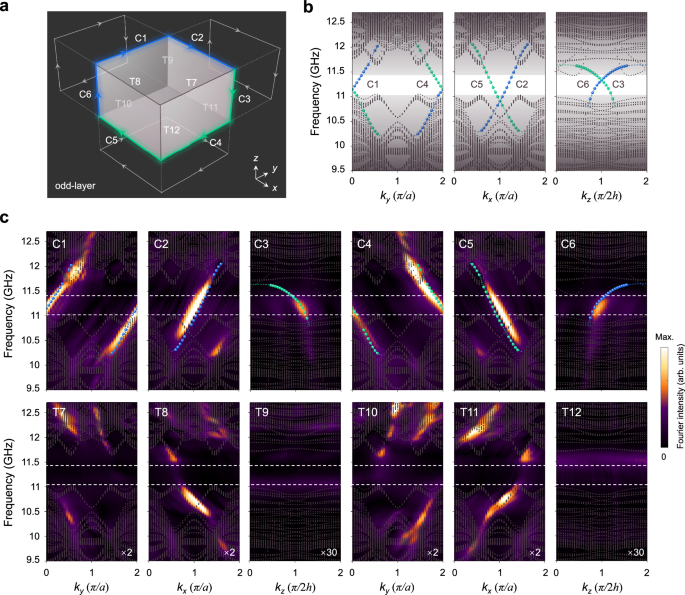
a Schematic of chiral hinge transport and its projections on different planes. Both the bottom and top layers are A-layer. Blue (green) arrow lines indicate energy flow along the positive (negative) directions of axes. All twelve hinges are labeled, i.e., C1-C6 chiral hinges and T7-T12 trivial hinges in this case. b Calculated projected band structures. Blue and green dots represent the corresponding chiral hinges. Black dots denote the projected bulk and surface states (shadow regions). c Measured dispersions of hinge states. Color scale represents the intensity. White dashed lines enclose the frequency window of the complete bulk and surface bandgap. For comparison, under the same color bar, the trivial hinge states (lower panels) are enlarged twice or thirty times (white numbers), corresponding to their chiral counterparts.
The numerically calculated hinge states are shown in Fig. 3b. The blue and green dots in each panel belong to diagonal hinges of two separate surfaces, different from coplanar edge states in either 2D quantum anomalous or quantum spin Hall materials. Such a pair of hinge states relates to each other under inversion symmetry, with the energy flowing along or facing the principal axis. For example, the negative slope of hinge dispersion of C4 suggests the wave propagating along the negative x direction, and vice versa for its counterpart hinge C1. The trivial hinges are gapped.
The shared complete bandgap frequency window for chiral hinge states is 11–11.4 GHz, with ~3.6% relative bandwidth. The experimentally measured hinge dispersions, as color scale shown in Fig. 3c, are in good agreement with the theoretical results (blue and green dots). Hinges C1-C6 behave in gapless yet one-way chiral manners, shaping in a non-coplanar closed chiral loop. Meanwhile, no observable states for hinges T7-T12 are found in the bandgap region. The corresponding transmission spectra are measured for twelve hinges as well to demonstrate their non-reciprocal characters (See Supplementary Fig. 2).
To get a momentum resolution of less than 0.1\(\pi\), we experimentally probe 21 periods along each direction in three divided samples to save materials (See “Methods” and Supplementary Fig. 3). It also should be noticed that the lateral surfaces are slightly modified here to increase the complete bandgap, benefiting the measurements of chiral hinge states (See Supplementary Figs. 4–5). The bandgap width for the z-axis chiral hinge states (C3 and C6) shrinks slightly due to the influence of trivial hinge states (right panel of Fig. 3b), which could be removed after further boundary decoration (See Supplementary Fig. 6). We also numerically calculate the surface Dirac masses and related surface Chern numbers for our photonic AXI (See Supplementary Fig. 7), agreeing with those in Fig. 1c.
Non-coplanar chiral hinge transport
Figure 4a shows the simulated hinge transport along the C6-C1-C2 route at the frequency of 11.2 GHz, excited at the V6 vertex, where the frontal (100) and bottom (001) planes are set to be absorptive surfaces to suppress the other three chiral hinge states. Although such a compact photonic AXI only contains 5 periods in x-y plane and 11 layers along z-axis (the same as Fig. 2a), we can unambiguously observe the non-coplanar hinge transport. The electromagnetic fields are mainly localized around the hinge.
Fig. 4: Non-coplanar and non-reciprocal hinge transport.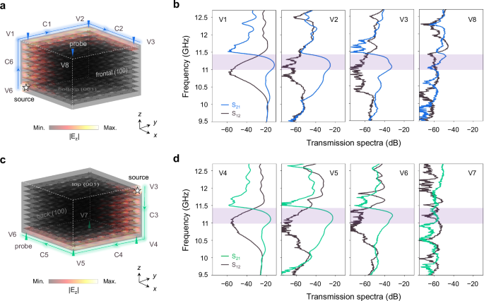
a Simulated chiral hinge transport along \({{\rm{C}}}6\)-C1-C2 route at the frequency of 11.2 GHz, using the V6 vertex excitation. All eight vertices are labeled from V1 to V8. The frontal (100) and bottom (001) facets are absorptive, while the copper plates cover the others. b Measured transmission spectra at V1–V3 and V8 vertices. Highlight regions denote the complete bandgap. c The case of C3-C4-C5 chiral route, using the V3 vertex excitation. The back (100) and top (001) facets are absorptive. d Transmission spectra at V4–V7 vertices.
We detect the forward and backward transmission spectra at four corners of the top (001) facet (Fig. 4b) in experiment (See Supplementary Fig. 8 for experimental sample). Since the chiral route crosses V1–V3 vertices, we can observe the high-efficient and non-reciprocal transport within the complete bandgap. But for the V8 vertex outside of the chiral route, both S21 and S12 parameters remain at low values. The case for hinge transport along the C3-C4-C5 route is displayed in Fig. 4c, d, showing the similar non-coplanar and non-reciprocal hinge transport.
In experiments, the frequency window for chiral hinge states is much broader than the complete bandgap. The non-reciprocal hinge transmission still works from 10.3 to 11.4 GHz (Fig. 4b, d), which has ~10% relative bandwidth, also coinciding with the dispersions measured in directional bandgaps shown in Fig. 3c. Besides the inevitably intrinsic loss, the gradually weakening S21 parameters (V1–V3 and V4–V6) are possibly attributed to the finite size. The electromagnetic waves could be scattered into the surface or bulk when meeting corners. We also verify that our non-coplanar chiral hinge transport is robust against various defects (See Supplementary Fig. 9). The experimental results for closed loop route of chiral hinge transport refer to Supplementary Fig. 10.
Tunability of chiral hinge states
The hinge states may exhibit varying performance in the even-layer scenario. In this case, the rigorous inversion symmetry for hinges is absent after considering boundaries, e.g., bilayer AB stacking. However, the rotation symmetry \(\left\{{2}_{\bar{1}10}|00(z/2)\right\}\) is restored. Since the even-layer (e.g., 14-layer) configuration can be regarded as the removal of just one top layer from the odd-layer (e.g., 15-layer) case, the lateral and bottom chiral hinge states (C3-C6) remain unchanged as those in Fig. 3, while the surface Dirac mass term of the top facet now becomes negative \(({m}_{001} \, . Under the restriction of rotation symmetry, hinges 7 and 8 become chiral hinges (relative to C5 and C4), while hinges 1 and 2 return trivial ones (relative to T11 and T10) at the current case (Fig. 5a).
Fig. 5: Even-layer scenario.
a Schematic of chiral transport in the 14-layer case. The top (bottom) layer is B-layer (A-layer). Hinges 7-8 are chiral (C7-C8), while hinges 1-2 are trivial (T1-T2). b Measured hinge dispersions (color scale). The bandgaps are delineated by white dashed lines.
The corresponding hinge dispersions of the top facet for a 14-layer photonic sample are measured in experiments (Fig. 5b), and they agree well with the above analysis and calculated results. If we add an additional B layer up to the bottom, it recasts to the odd-layer photonic AXI case, but with the BAB configuration different from those in Fig. 3a, equivalent to flip magnetic fields. Then, the chiral loop changes to be C6-C8-C7-C3-C11-C10. In all the cases mentioned above, hinges C3 and C6, restricted by the mirror plane of the glide symmetry, are kept unchanged. Their wave flow directions can still be reversed when exchanging AB and BA interlayers. Moreover, we could also tune hinges T9 and T12 (C3 and C6) into chiral (trivial) by rotating the T-shirt-like hollow holes in Fig. 2a.