The Stochastic Processing Unit
We now introduce our stochastic processing unit (SPU), which is depicted in the left panel of Fig. 1. The SPU is constructed on a Printed Circuit Board. From the lower left corner to the upper right corner, one can see the line of components corresponding to eight unit cells (LC circuits), while the components arranged in the triangle on the upper left correspond to the controllable couplings that couple the unit cells. We remark that we constructed three nominally identical copies of our SPU circuit, to test the scientific reproducibility of our experimental results.
Fig. 1: The stochastic processing unit (SPU).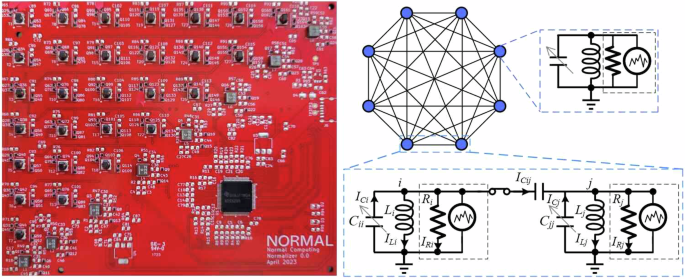
(Left panel) The Printed Circuit Board for our 8-cell SPU. (Right panel) Illustration of eight unit cells that are all-to-all coupled to each other, as in our SPU. Each cell contains an LC resonator and a Gaussian current noise source, as shown in the circuit diagram on the top right. The circuit diagram on the bottom depicts two capacitively coupled unit cells.
The SPU can be mathematically modeled as a set of capacitively coupled ideal RLC circuits with noisy current driving. The diagram for this model is shown in the right panel of Fig. 1. Doing a simple circuit analysis reveals that the equations of motion for this circuit are
$${{{\rm{d}}}}{{{\bf{i}}}}={{{{\bf{L}}}}}^{-1}{{{\bf{v}}}}\,{{{\rm{d}}}}t$$
(4)
$${{{\rm{d}}}}{{{\bf{v}}}}=-{{{{\bf{C}}}}}^{-1}{{{{\bf{R}}}}}^{-1}{{{\bf{v}}}}\,{{{\rm{d}}}}t-{{{{\bf{C}}}}}^{-1}{{{\bf{i}}}}\,{{{\rm{d}}}}t+\sqrt{2{\kappa }_{0}}{{{{\bf{C}}}}}^{-1}{{{\mathcal{N}}}}[0,{\mathbb{I}}\,{{{\rm{d}}}}t],$$
(5)
where \({{{\bf{i}}}}={\left({I}_{L1},\ldots {I}_{Ld}\right)}^{{{{\rm{T}}}}}\) is the vector of inductor currents and \({{{\bf{v}}}}={\left({V}_{C1},\ldots {V}_{Cd}\right)}^{{{{\rm{T}}}}}\) is the vector of capacitor voltages. In the above, C is the Maxwell capacitance matrix, whose diagonal elements are \({{{{\bf{C}}}}}_{ii}={C}_{ii}+\mathop{\sum }_{j=1}^{d}{C}_{ij}\), and whose off-diagonal elements are Cij = −Cij. The values of resistors and inductors in each cell are represented by the matrices \({{{\bf{R}}}}=R{\mathbb{I}}\) and \({{{\bf{L}}}}=L{\mathbb{I}}\) respectively. Finally, \({{{\mathcal{N}}}}[0,{\mathbb{I}}\,{{{\rm{d}}}}t]\) represents a mean-zero normally distributed random displacement with covariance matrix \({\mathbb{I}}\,{{{\rm{d}}}}t\) and κ0 is the power spectral density of the current noise source. In this implementation, in order for the noise amplitude to be of sufficient magnitude, the noise source is a controllable random bit stream generated by a digital controller (see Supplementary Information for more details). If the magnitude of the noisy driving current is larger than the intrinsic noise in the system, then κ0 can be thought of as an effective temperature control for thermodynamic computation.
Equations (4) and (5) can be mapped to the Langevin equations (1) and (2) by making a change of coordinates. Specifically, we introduce the magnetic flux vector ϕ and the Maxwell charge vector q, defined as
$${{{\boldsymbol{\phi }}}}=L{{{\bf{i}}}},\quad {{{\bf{q}}}}={{{\bf{C}}}}{{{\bf{v}}}}.$$
(6)
As shown in the Supplementary Information, ϕ and q are canonically conjugate coordinates, with ϕ playing the role of position and q playing the role of momentum. We also introduce an effective inverse temperature parameter \(\beta=\gamma {\kappa }_{0}^{-1}\). In terms of these variables, Eqs. (4) and (5) become
$${{{\rm{d}}}}{{{\boldsymbol{\phi }}}}={{{{\bf{C}}}}}^{-1}{{{\bf{q}}}}\,{{{\rm{d}}}}t$$
(7)
$${{{\rm{d}}}}{{{\bf{q}}}}=-{L}^{-1}{{{\boldsymbol{\phi }}}}\,{{{\rm{d}}}}t-{R}^{-1}{{{{\bf{C}}}}}^{-1}{{{\bf{q}}}}\,{{{\rm{d}}}}t+{{{\mathcal{N}}}}[0,2{R}^{-1}{\beta }^{-1}{\mathbb{I}}\,{{{\rm{d}}}}t].$$
(8)
It is clear that Eqs. (7) and (8) are equivalent to (1) and (2) when we make the identifications x = ϕ, p = q, M = C, γ = R−1, and \(U({{{\bf{x}}}})=U\left({{{\boldsymbol{\phi }}}}\right)=\frac{1}{2}{{{{\boldsymbol{\phi }}}}}^{T}{{{{\bf{L}}}}}^{-1}{{{\boldsymbol{\phi }}}}\). In these coordinates, the Hamiltonian, without noise or dissipation, of the system is expressed as
$${{{\mathcal{H}}}}\left({{{\boldsymbol{\phi }}}},{{{\bf{q}}}}\right)=\frac{1}{2}{{{{\boldsymbol{\phi }}}}}^{T}{{{{\bf{L}}}}}^{-1}{{{\boldsymbol{\phi }}}}+\frac{1}{2}{{{{\bf{q}}}}}^{T}{{{{\bf{C}}}}}^{-1}{{{\bf{q}}}},$$
(9)
and consequently, the stationary distribution of Eqs. (7) and (8) is the Gibbs distribution given by
$${{{\boldsymbol{\phi }}}} \sim {{{\mathcal{N}}}}[0,{\beta }^{-1}{{{\bf{L}}}}],\quad {{{\bf{q}}}} \sim {{{\mathcal{N}}}}[0,{\beta }^{-1}{{{\bf{C}}}}],$$
(10)
where ϕ and q are independent of each other.
The time to reach the Gibbs distribution, the equilibration time, is closely related to the correlation time τcorr, since equilibration can be interpreted as the decorrelation of the system from its initial state. So the two timescales are essentially the same. While sampling at a rate given by the inverse correlation time of the system is a guarantee of uncorrelated samples, in practice, one can sample much faster and retain good performance, see Supplementary Information for details. For our SPU, the correlation function decays exponentially with a time constant of approximately
$${\tau }_{{{{\rm{corr}}}}}\approx R{c}_{\max },$$
(11)
where \({c}_{\max }\) is the largest eigenvalue of C (see, e.g., ref. 16). (There are some minor corrections involving the other circuit parameters, but these have relatively little effect.) In order for the correlation function to decay to less than one percent of its original magnitude, we may wait for an interval of at least 5τcorr, for example. If one periodically measures the voltages, v, across the capacitors after the device has reached equilibrium, one finds that the voltage samples will have a covariance matrix of
$${{{{\mathbf{\Sigma }}}}}_{{{{\bf{v}}}}}=R{\kappa }_{0}{{{{\bf{C}}}}}^{-1}.$$
(12)
We now describe how this computing system can be used for various mathematical primitives.
Gaussian sampling
Let us describe how to perform Gaussian sampling with our thermodynamic computer. Consider a zero mean multivariate Gaussian distribution (since we can always translate the samples by a constant vector to generate a non-zero mean):
$${{{\mathcal{N}}}}({{{\bf{x}}}}| {{{\mathbf{\Sigma }}}})=\frac{1}{\sqrt{{(2\pi )}^{N}| {{{\mathbf{\Sigma }}}}| }}\exp \left(-\frac{1}{2}{{{{\bf{x}}}}}^{T}{{{{\mathbf{\Sigma }}}}}^{-1}{{{\bf{x}}}}\right),$$
(13)
where Σ is the covariance matrix. Here, we consider the case where the user provides the precision matrix P = Σ−1 associated with the desired Gaussian distribution (See Supplementary Information for the alternative case where the user provides the covariance matrix Σ.)
As described above, the stationary distribution of the voltages and currents in the SPU is dependent on the noise- and dissipation-free Hamiltonian of the circuit. The Hamiltonian for the coupled oscillator system (see Supplementary Information for details) is given by:
$${{{\mathcal{H}}}}\left({{{\bf{i}}}},{{{\bf{v}}}}\right)=\frac{1}{2}{{{{\bf{v}}}}}^{T}{{{\bf{C}}}}{{{\bf{v}}}}+\frac{1}{2}{{{{\bf{i}}}}}^{T}{{{\bf{L}}}}{{{\bf{i}}}},$$
(14)
where i is the vector of currents through the inductors in each unit cell, v is the vector of voltages across the capacitors in each unit cell, C is the Maxwell capacitance matrix, and L is the inductance matrix.
At thermal equilibrium, the dynamical variables are distributed according to a Boltzmann distribution, proportional to \(\exp (-{{{\mathcal{H}}}}/kT)\), and hence v is normally distributed according to:
$${{{\bf{v}}}} \sim {{{\mathcal{N}}}}[{{{\bf{0}}}},kT{{{{\bf{C}}}}}^{-1}]$$
(15)
Thus, if the user specifies the precision matrix P, then we can obtain the correct distribution for v by choosing the Maxwell capacitance matrix to be:
$${{{\bf{C}}}}=kT{{{\bf{P}}}}$$
(16)
Hence, this describes how we can map the user-specified matrix to the matrix of electrical component values, to obtain the desired distribution.
Figure 2 is a visualization of a Gaussian sampling experiment performed on our SPU (here, the data from two unit cells is reported, see the Supplementary Information for the rest of the results). One can see good agreement with the theoretical distribution and its marginals. One can also see that the the error associated with the moments of the distribution goes down over time as more samples are gathered.
Fig. 2: Sampling a two-dimensional Gaussian distribution on the SPU.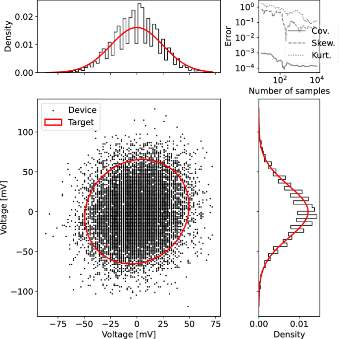
Measurements of the voltages of two coupled cells of the SPU were taken at a rate of 12 MHz. Top Left: histogram of the marginal of cell i. Top right: Absolute error between the target covariance matrix and the device covariance matrix (abbreviated as Cov.), similarly for the skewness and kurtosis (respectively abbreviated as Skew. and Kurt.), all calculated using the Frobenius norm. Bottom Left: Scatter plot of voltage samples from both cells. Bottom Right: Histogram of the marginal of cell j. For the marginal plots, the theoretical target marginal is overlaid as a solid red curve. Similarly, for the two-dimensional plot, the theoretical curve corresponding to two standard deviations from the mean is overlaid as a solid red curve. Source data are provided as a Source Data file.
Matrix inversion
The second primitive we will consider is matrix inversion, which was discussed in the context of thermodynamic computing in ref. 16. Following that reference, we envision the user encoding their matrix A in the precision matrix P of the associated Gaussian distribution that will be sampled. Hence from Eq. (16), the Maxwell capacitance matrix of the hardware is given by C = kTA. Choosing this Maxwell capacitance matrix, we find from Eq. (15) that at thermal equilibrium, the voltage vector is distributed according to
$${{{\bf{v}}}} \sim {{{\mathcal{N}}}}[{{{\bf{0}}}},{{{{\bf{A}}}}}^{-1}]$$
(17)
Therefore, we can invert matrix A simply by collecting voltage samples at thermal equilibrium and computing the sample covariance matrix. (This assumes that A is a positive semi-definite (PSD) matrix, although the extension to non-PSD matrices is possible with a pre-processing step16).
Figure 3 shows the 8 × 8 matrix inversion results. We perform the algorithm on three distinct copies of the SPU, which are nominally identical (although may slightly differ due to component tolerances). The fact that similar results are obtained on all three SPUs, as shown in Fig. 3A, is useful for demonstrating scientific reproducibility. Indeed, one can see the error (i.e., the relative Frobenius error between the SPU inverse and the target inverse) goes down as the number of samples increases. The SPU inverse, after gathering several thousand samples, looks visually similar to the target inverse. Moreover, Fig. 3B shows the time evolution of the SPU inverse. One can see in Fig. 3B that the SPU inverse gradually looks more-and-more like the true inverse as more samples are gathered.
Fig. 3: Thermodynamic inversion of an 8 × 8 matrix.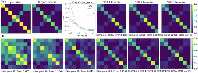
This experiment was performed independently on three distinct (but nominally identical) copies of the SPU. A The input matrix A and its true inverse A−1 are shown, respectively, in the first and second panel. The relative Frobenius error versus the number of samples is plotted in the third panel, for each of the three SPUs. The three panels on the right show the experimentally determined inverses after gathering 12,000 samples on each of the three SPUs. B The time progression of thermodynamic matrix inversion is shown. From left to right, more samples are gathered from the SPU to compute the matrix inversion. The number of samples and the inversion error are stated below each panel. One can visually see the resulting inverse look more like the target inverse as more samples are obtained. Source data are provided as a Source Data file.
The fact that the error does not go exactly to zero indicates that experimental imperfections are present. This likely includes capacitance tolerances (i.e., nominal capacitance values being off from their true values) and imprecision. We recently showed that the latter can be addressed with a judicious averaging protocol, and the experimental error for matrix inversion can be significantly reduced32. Thus, imprecision-based errors can be mitigated for this system.
In the Supplementary Information, we show some additional plots for matrix inversion on our SPU, including the dependence of the error on the condition number of A and on the smallest eigenvalue of A.
Performance advantage at scale
We now focus on the potential advantage that one could obtain from scaling up our SPU. Specifically, we compare the expected runtime and energy consumption of our SPU to that of state-of-the-art GPUs. Our mathematical model for runtime and energy consumption involves considering the effect of three key stages:
-
1.
Calculating the component values of the capacitor array from the input covariance matrix (digital calculation, on a GPU)
-
2.
Loading the component values to the device (digital transfer)
-
3.
Waiting for the integration time of the physical dynamics needed to generate the samples (analog runtime).
-
4.
Sending the samples back to the digital device through an ADC.
We assume the SPU is constructed from standard electrical components operating at room temperature and the ideal case of electrical components with 16 bits of precision, as well as that the SPU units are fully connected (This analysis is valid whether the user provides the covariance matrix or the precision matrix, where details of sampling when the covariance matrix is provided is discussed in Supplementary Information.) We assume the following:
-
The physical time constant of the system is 1μs.
-
The number of ADC channels scales with dimension, with a sampling rate of 10 Megasamples per second.
-
The power per cell is 0.005 mW, dominated by ADC power consumption.
For comparison with digital state-of-the-art, we obtain digital timing and energy consumption results using a JAX implementation of Cholesky sampling on an NVIDIA RTX A6000 GPU using the package zeus – ml33.
Figure 4a shows how the time taken to produce samples from a multivariate Gaussian scales with dimension, for the cases of drawing 1 sample and drawing 10,000 samples. We emphasize that this figure is relevant to both Gaussian sampling and matrix inversion, because one can always use the obtained samples to estimate the matrix inverse. Hence, the timing results shown in this figure apply to both Gaussian sampling and matrix inversion.
Fig. 4: Comparison of GPU and estimated SPU performance.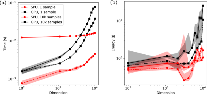
a Time to solution to obtain Gaussian samples for dimensions ranging from 100 to 10,000 for an A6000 GPU (black squares) and estimated for the SPU (red dots), for both a single sample (dashed lines) and 10,000 samples (solid lines). b Corresponding energy to solution, directly measured for the GPU and estimated for the SPU. Source data are provided as a Source Data file.
One can see that for 10,000 samples, the GPU is faster for low dimensions, but the SPU performance is expected to outperform the GPU for high dimensions. The cross-over point, which we call the point of “thermodynamic advantage”, occurs around d = 3000 for the assumptions we made. The asymptotic scaling for high dimensions is expected to go as O(d2) for the SPU, as opposed to O(d3) for Cholesky sampling on the GPU. At d = 10,000, an order-of-magnitude speedup is predicted, and larger speedups could be unlocked by scaling up the system to larger sizes.
For the case of drawing a single sample, we once again predict roughly an order-of-magnitude speedup for the SPU over GPUs at d = 10,000. However, what is different about this case is that a speedup is predicted over the entire range of dimensions considered, with a small speedup even being predicted at low dimensions (e.g., d = 100). The large difference in SPU runtime (between the single sample and 10,000 sample cases) is because the runtime is dominated by the ADC conversion, which is greatly reduced in the case of a single sample.
It is also of interest to consider energy, since it is well known that GPUs consume large amounts of energy. In contrast, the natural dynamics of a physical system are energy-frugal and could reduce the expected energy requirements. Figure 4b shows how the energy of generating Gaussian samples is expected to scale with dimension for both the SPU and GPU. (Note that a large variance is observed for energy because of the direct measurement of GPU operations for both the GPU and SPU benchmarks.) One can see that our model predicts the exciting prospect that the SPU provides energy savings for all dimensions, even for low dimensions. Moreover, the energy savings is an order of magnitude at d = 10,000 and is expected to continue to grow for larger dimensions.
It is encouraging that a simple model of the SPU, the timings involved in its end-to-end operation, and the energy cost during these processes lead to a potential speedup and energy savings of more than an order-of-magnitude relative to state-of-the-art GPUs with relatively conservative assumptions. Nevertheless, these results represent a mathematical model, and the true evidence of thermodynamic advantage will only be obtained by directly scaling up the SPU hardware.
A scalable architecture
An important lesson learned from the small-scale proof-of-concept experiments reported above is that the architecture we employed would not be the best choice for a large-scale implementation that would require miniaturization as an integrated circuit (IC). Firstly, the presence of inductors and transformers makes an IC implementation very difficult due to, e.g., the physical size of the inductors and their relatively strong parasitic coupling and crosstalk at those scales34,35. Secondly, area constraints on an IC would likely require the capacitances to be very small (particularly for high dimensions), leading to a very short RC time constant. Therefore, the noise must have a very large bandwidth to match the timescale of the system’s dynamics.
We propose here an alternative architecture that is better suited to overcome these issues of large-scale implementation. The proposed architecture uses RC unit cells and resistive coupling and is shown as a 2-dimensional example in Fig. 5a. A detailed analysis of the dynamical equation for this circuit is given in the Supplementary Information. Clearly, this architecture eliminates scaling issues related to inductors. Moreover, our numerical benchmarks of this architecture (provided in the Supplementary Information) involving a mathematical model for runtime and energy consumption show a similar speedup and energy advantage as that shown in Fig. 4. Hence, the advantage can be preserved while switching to a more scalable architecture.
Fig. 5: Architecture with resistive coupling.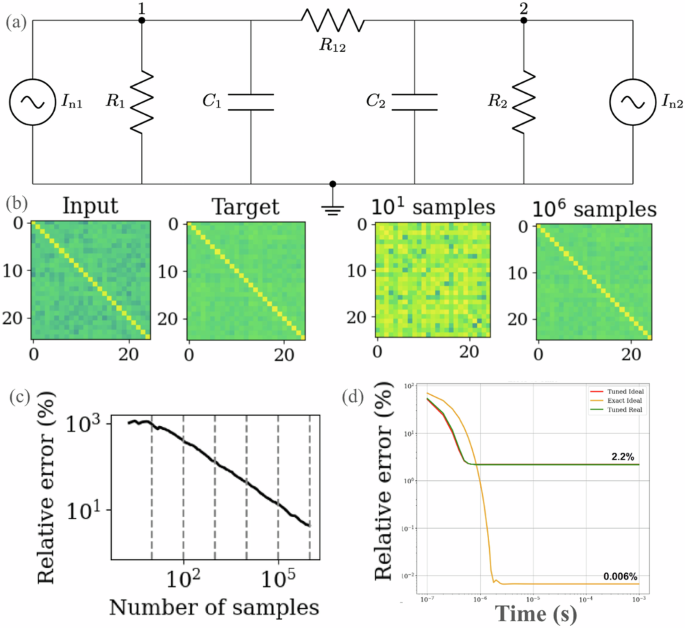
a Circuit diagram for two unit cells of the proposed architecture with resistive coupling. b SPICE simulations of matrix inversion for d = 25 with this architecture, showing qualitative agreement between the target and the experimentally determined inverse. c For this SPICE simulation, the relative error is plotted versus the number of samples. d CADENCE simulations for d = 20 unit cells with the resistively coupled architecture are shown, plotting the relative error versus time. The three curves correspond to the case where all components are ideal and have the exact value needed (orange), the case where all components are ideal, but where the resistances are composed of 8-bit banks of resistors (red), and the case where all the components are simulated with non-idealities given by the fabrication models (green) and the resistances are composed of 8-bit banks. Source data are provided as a Source Data file.
We further confirm the performance of this circuit by running SPICE simulations shown in Fig. 5b. In this simulation, 25 unit cells are densely connected by an array of resistors to calculate the inverse of a 25 × 25 matrix. Figure 5c shows the relative error of the inverse matrix calculated by the circuit simulation and the target inverse as a function of the number of voltage measurements. We can see that this circuit behaves as expected, and the stationary distribution is indeed a normal distribution with covariance equal to the inverse of the conductance matrix.
To account for the impact of non-idealities, we ran Cadence simulations, shown in Fig. 5d. This simulation, for d = 20 unit cells, fully accounts for realistic hardware components using component models from the fabrication foundry as well as quantization error by implementing the tunable resistances (conductances) as banks of multiple resistors that can be individually addressed. The green curve in this plot represents the most realistic case where all the components have real models and all coupling elements are implemented using 8-bit resistor banks. The asymptotic error is still reasonable (~2%) despite accounting for non-idealities, suggesting that this architecture has the potential to perform well in a realistic setting. This study of fabrication-based non-idealities reveals that fabrication defects are not dominant compared to the quantization error. We remark that this provides hope for employing quantization-based error mitigation methods32 to reduce overall error. Finally, in the Methods section, we provide detailed timing and energy benchmarks from our Cadence simulations as a function of dimension, showing how the energy costs, runtime, and area on chip increase with dimension.