Our density-functional theory (DFT) suggests that BP intercalated with a few percent of Co (See schematics in Fig. 1a) can be FM33,34,35 (Supplementary Notes 1–2). Here, the hybridization with native p-derived bands of BP is minor, so the intercalated Co atoms induce little charge transfer to BP, preserving its ambipolar gate-tunability. We define “majority” and “minority” spin states as the population imbalance between spin-up and spin-down states in Co-BP relative to Co electrode. Figure 1b presents the corresponding DOS schematic for Fig. 1c. In addition, in the conduction band, the population of spin-up is equal to that of spin-down (quenched magnetic moments). But near the conduction band edge, there exists a localized magnetic state. This state can be probed with tunnelling experiments. Inside the gap, there is no accessible state. On the other hand, in the valence band, there is an imbalance of spin-up and spin-down states. This gives rise to alternating behaviour of majority and minority carries as a function of \({E}_{{{{\rm{F}}}}}\). We note that the electric-field tunability in BP also depends on Co doing concentration (See Supplementary Fig. S1).
Fig. 1: Structural and electronic properties of Co-doped BP.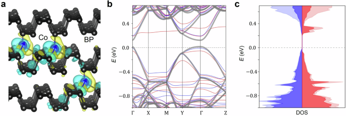
a Atomic structure of the Co-intercalated BP illustrating magnetic doping in this system. Spin density isosurfaces of the Co atoms support an FM order in Co-BP. b Spin-polarized band structure of the same supercell after intercalation of a Co atom (3%) between the phosphorene layers; blue (red) represents the spin-up and spin-down bands. The grey curves represent the bands of pristine bulk BP. c Calculated density of states (DOS) of Co-BP near the Fermi level (\({E}_{{{{\rm{F}}}}}\)(0)) according to the bandstructure of the charge neutral configuration shown in (b). Blue and red bands represent spin-up and spin-down, respectively. Dashed line is the \({E}_{{{{\rm{F}}}}}\). Light colours represent the total DOS, while dark colours show only the d orbital projected DOS.
First, we confirm the feasibility of implanting Co atoms in BP using planar-view atomic-resolution scanning transmission electron microscopy (STEM) (See Fig. 2a, b, Supplementary Fig. S2 and Methods). We achieve average Co doping concentration and Co separation of ~3% and ~2 nm, respectively, and do not detect signatures of Co clustering or other defects (confirmed with four separate samples). To confirm the semiconducting nature of our Co-BP (See the optical micrograph and measurement set-up in Fig. 2c), we measure current under constant bias voltage (\({V}_{{{{\rm{SD}}}}}=\,\)−1 V) and back-gate voltage \({V}_{{{{\rm{g}}}}}\) varying from −75 V to +100 V. A clear OFF state is visible for \({V}_{{{{\rm{g}}}}}\) range between 0 V and 36 V. Beyond this range, our device shows bipolar behaviour with hole mobility up to 1000 \({{{{\rm{cm}}}}}^{2}{{{{\rm{V}}}}}^{-1}{{{{\rm{s}}}}}^{-1}\) and an ON/OFF ratio exceeding 5000 (Top panel in Fig. 2d). This suggests that our Co-BP remains charge neutral (or slightly p-type) and thus can be tuned into either n-type or p-type by the back gate.
Fig. 2: Anomalous Hall effect and anisotropic magnetoresistance of Co-BP.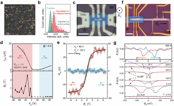
a Planar-view atomic-resolution HAADF image of a Co-doped multilayer BP flake. The image intensity is directly related to the atomic weight of the imaged species. The brightest spots in the planar view HAADF image (marked with red circles) are isolated Co atoms on the BP surface while the dimmer spots (yellow circles) show isolated Co atoms intercalated in deeper interlayer spaces. b Intensity histogram of the mapped atomic columns in (a), indicating the adsorbed and intercalated individual Co atoms with P atomic columns. c Optical micrograph and measurement schematics of the lateral Hall bar device (Device A) of Co-BP on 285-nm SiO2/Si substrate. The ultra-thin BN acts as an encapsulation/diffusion barrier that protects BP and allows dilute Co intercalation. Pairs of Ti/Au (2/85 nm) contacts labelled by #1 and #2 and by #1 and 3 are used for probing the Hall resistance (\({R}_{{xy}}\)) and the channel resistance (\({R}_{{xx}}\)), respectively under a constant current from source (S) to drain (D). Scale bar: 4 μm. d Top panel: Transconductance of the lateral Hall bar device at \({V}_{{{{\rm{SD}}}}}=\) −1 V. Bottom panel: The magnetization field (\({B}_{{{{\rm{C}}}}}\)) as a function of back-gate voltages. The error bars are extracted by fitting with a confidence interval of 99.7%. e Two representative anomalous Hall effect curves at 1.6 K in the hole regime (red dots, fitted by the black line) and electron regime (blue dots). f Optical micrograph and schematics of Device B for in-plane MR measurement. The MR is probed by the voltage between the contacts labelled by #1 and #2. The injection electrode is made of Co/Ti (1.5 nm/35 nm), where Co was deliberately deposited as a discontinuous dust layer of 1.5-nm nominal thickness. Scale bar: 3 μm. g Temperature dependence of MR at \({V}_{{{{\rm{g}}}}}=\) − 50 V and Ibias = −40 μA. For comparison, the bottommost curve (black) refers to the metallic electrode (Co/Ti) itself at \(T=\) 2.5 K, confirming it has no magnetoresistance. The in-plane field (\({B}_{{||}}\)) is collinear with the current. The zoomed-in details of the MR at 300 K are shown in the top panel.
Next, we investigate the magnetic nature of our Co-BP by performing AHE measurements (Device A, See Methods). We sweep an out-of-plane magnetic field (\({B}_{\perp }\)) and show the representative \({R}_{{{{\rm{xy}}}}}-{B}_{\perp }\) curves in hole and electron regimes (Fig. 2e). In the hole regime, the field dependence can be described by a Langevin-type function \({R}_{{xy}}^{{{{\rm{AHE}}}}}={R}_{0}^{{{{\rm{AHE}}}}}\tanh \left(\frac{B}{{B}_{{{{\rm{C}}}}}}\right)\)36, where \({R}_{0}^{{{{\rm{AHE}}}}}\) is proportional to the saturation magnetization and \({B}_{{{{\rm{C}}}}}\) is the saturation field (See the fitting in Fig. 2e). This suggests magnetism in Co-BP (See the extracted \({B}_{{{{\rm{C}}}}}\) in bottom panel of Fig. 2d and details in Supplementary Fig. S3). In contrast, we do not observe any AHE with a positive back gate, possibly because the lateral transport cannot probe the expected magnetic order near the conduction band minimum due to low conductance. This regime will be examined in the vertical tunnelling Devices C and D below, which is less sensitive to the low conductivity at the conduction band edge.
To corroborate the FM order in Co-BP, we compare its in-plane MR with a Co-dust film alone of the same evaporated thickness (~1.5 nm). Both geometries are shown in Fig. 2f (Device B, See Methods) and are capped by a Ti layer, since Co dust alone is non-conducting. We sweep the in-plane field (\({B}_{{{{\rm{||}}}}}\)) along the direction of the applied current along the zig-zag direction (See Supplementary Fig. S4). The absence of MR in “Co dust + Ti” electrode (probed with contacts labelled by “3” and “4”) strongly suggests the lack of FM long-range order in Co dust itself (curve labelled “Co dust” in Fig. 2g). In contrast, the Co-doped BP region (probed with contacts labelled by “1” and “2”) displays very large and hysteretic MR, as reflected in the longitudinal field sweeps at various temperatures up to 300 K shown in Fig. 2f. This is characteristic of a FM channel undergoing magnetization reversal as a function of a collinear magnetic field sweep37. Both \({B}_{{{{\rm{C}}}}}\) and \(\Delta R\) are finite, indicating that Co-BP remains FM beyond room temperature.
To further characterize the magnetism in Co-BP, we perform magneto-optic Kerr effect (MOKE) measurements at room temperature. We note that the Co dusts are also evaporated on adjacent Au pads to compare the differences in MOKE signals. In Co-BP, the out-of-plane polar MOKE signal is large, negative, and saturates at 700 mT. As expected, the saturation field at room temperature is smaller than that measured by the AHE at 1.6 K. Since the sample is slightly tilted, there is a small in-plane magnetic field component, allowing us to also record simultaneously the in-plane MR (See Methods). We observe an in-plane MR signal with a switching field that matches that of the MOKE signal originating from the initial in-plane reversal of the magnetization (blue region in Fig. 3a). It is also comparable to that observed in the in-plane MR measurements shown in Fig. 2g. In contrast, MOKE measurements of Co dust on Au electrodes exhibit none of these features. Instead, only a small kink near zero field indicative of disconnected Co clusters is observed (Fig. 3b).
Fig. 3: MOKE and MFM characterizations of the Co-BP device.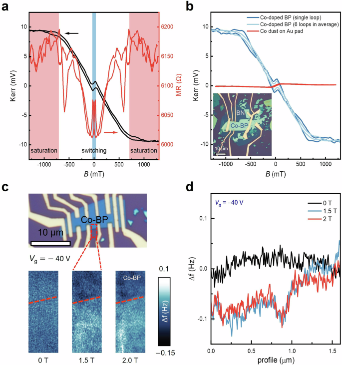
a Kerr signal and MR signal. Blue region indicates the in-plane switching and the orange region indicates the out-of-plane saturation during the field scan. b A comparison of Kerr signals on Co-BP and Co on Au pads. Inset: Optical micrograph showing the Co-BP region. c MFM characterization of the sample at 1.7 K and under \({V}_{{{{\rm{g}}}}}=\) − 40 V. At, as \({B}_{\perp }\) increases, a darker region (the edge is denoted by the dashed line) begins to appear in the Co-BP region. This corresponds to a negative frequency shift (Δf) that represents an attractive force between the cantilever and sample surface, indicating Co-BP becomes magnetic. d MFM profiles of the line scans for frequency shift (Δf) from c. The curves are shifted vertically for better presentation.
We also performed magnetic force microscopy (MFM) measurements (Methods & Supplementary Information). Here, we evaporate Co dusts onto the entire substrate such that we can compare the MFM signals from Co-BP and Co-SiO2 (See the labelled region in the micrograph from in Fig. 3c). We record the frequency shift (Δf) as a function of position (Fig. 3c) at 1.7 K. A large Δf is due to the attractive force between the magnetic cantilever and a magnetic substrate. In our experiments, we only observed such a magnetic signature for Co-BP at negative gate voltages and absent on the SiO2 substrate. Here, we discuss representative data at \({V}_{{{{\rm{g}}}}}=-\)40 V. At zero magnetic field, no magnetic signal is observed. As the magnetic field increases, Δf increases in the Co-BP defined by the darker region with a well-defined edge (top part of the scan). On the other hand, Δf on the SiO2 region remains unchanged. At magnetic fields above 1.5 T, similar to the AHE measurements in Fig. 2c, the magnetic contrast saturates. Additionally, we show representative line scans of Δf in Fig. 3d. The difference in Δf between the scans at 0 T and 1.5 T is clearly visible in the Co-BP region (~0.1 Hz) but marginal on SiO2.
From an application perspective, an important question is whether Co-BP can be easily integrated into ready-to-use spintronic devices with gate tunability. Here, our proof-of-concept device is a magnetic tunnel junction (MTJ), which uses Co-doped BP layer and a 35-nm thick Co stripe act as the ferromagnetic layers with BN as the tunnelling barrier (Devices C and D in Fig. 4a) (See Methods and Supplementary Fig. S5). Intriguingly, we observe hysteretic switching between two distinct resistance states in the TMR when sweeping \({B}_{{{{\rm{||}}}}}\) along the easy axis of the Co contact. A representative TMR measurement at \(T=\) 2.5 K shown in Fig. 4b displays well defined, large resistance steps (∆R = 800 Ω, upper panel). In addition, the minor loop (lower panel) displays the square-shaped hysteretic profile expected for an FM–insulator–FM MTJs, thus confirming the existence of an effective FM contact on the BP side of the junction with a well-defined coercive field.
Fig. 4: Tunnelling characteristics of vertical Co/BN/BP devices.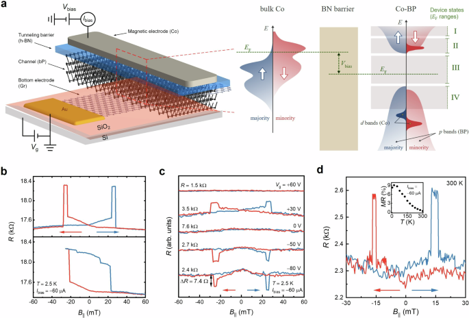
a Left panel: Schematic drawing of the vertical Co/BN/BP MTJ devices studied in this work, which are grounded by a bottom-contacted graphene electrode. Right Panel: Schematic spin-resolved density of states of bulk Co (left) and of Co-BP (right) qualitatively reflects the DFT + U band structures. For Co-BP, the light-shaded red and blue areas represent the phosphorus p-derived bands, only slightly changed relative to pristine BP; the darker, peaked traces represent the narrow bands associated with the Co d orbitals. The energy ranges labelled I–IV refer to the corresponding device operation states discussed in the text. b Major (upper panel) and minor (lower panel) loop scans of the tunnelling magnetoresistance (TMR) of TMJ (Device C) under \({V}_{{{{\rm{g}}}}}=+ 20\) V at 2.5 K, with magnetic field parallel to the top Co electrode. c TMR of Device D at different gate voltages (\({V}_{{{{\rm{g}}}}}\)), measured at 2.5 K with \({I}_{{{{\rm{bias}}}}}=\) − 60 μA (DC) + 5 µA (AC). From top to bottom: Co-BP becomes increasingly p-type with the positive-to-negative \({V}_{{{{\rm{g}}}}}\) variation; background resistances are 1.5, 3.5, 7.6 and 2.7 kΩ, respectively (at \({B}_{{||}}=\) −60 mT). d TMR under Ibias= − 60 A (DC) + 5 µA (AC) in Device C at 300 K. Inset: The temperature dependence of TMR. The data are extracted from Supplementary Fig. S6.
We then demonstrate the gate-tunability of the Co-BP DMS (Fig. 4c). The measurements reveal a sequence of four “operational states”, namely, an absence of TMR in n-type BP (\({V}_{{{{\rm{g}}}}}=\) + 60 V), a positive TMR near the edge of conduction band (\({V}_{{{{\rm{g}}}}}=\) + 30 V), an absence of TMR inside the gap (\({V}_{{{{\rm{g}}}}}=0{V}\)), a negative TMR p-type BP (\({V}_{{{{\rm{g}}}}}=-50\,\)V). Specifically, we labelled these four states as I–IV with reference to the corresponding energy ranges highlighted in the DOS schematic of Co-BP shown in Fig. 4a. Here the position of \({E}_{{{{\rm{F}}}}}\) in Co-BP determines whether the local moments \({{{{\boldsymbol{\mu }}}}}_{{{{\rm{Co}}}}}\) are finite or zero, allowing gate control of local moment formation. Specifically, in device state I, Co-BP is a n-type semiconductor with \({E}_{{{{\rm{F}}}}}\) in the conduction band and quenched moments, explaining the featureless MR curve at \({V}_{{{{\rm{g}}}}}\ge\) + 50 V. In device state II, \({E}_{{{{\rm{F}}}}}\) lies near the band edge and \({{{{\boldsymbol{\mu }}}}}_{{{{\rm{Co}}}}}\) is finite, so that Co-BP is FM and the heterostructure operates as a tunnelling spin valve that probes the localized magnetic moments from Co. In comparison, this state is not visible in lateral transport (i.e., Device A) mostly likely due to the marginal conductance at the conduction band edge38. Device state III is obtained upon further reducing \({E}_{{{{\rm{F}}}}}\) into the gap, in which case, the itinerant carrier density may now be insufficient to couple FM order among them. Further reducing \({V}_{{{{\rm{g}}}}}\) brings \({E}_{{{{\rm{F}}}}}\) to the valence band with a substantial increase in carrier density. In device state IV, unlike in the conduction band minimum, Co-BP is reinstated as a FM contact and the spin-valve signal re-emerges but is inverted. The opposite TMR sign in states II and IV is in good agreement with DFT which also sees an inversion of majority and minority spins in BP. The tunnelling out of the bulk Co electrode injects minority spin polarization into Co-BP; consequently, a positive (negative) TMR step will only arise when minority (majority) states are dominant on the Co-BP side. The electric field effect of BP not only allows for turning ON/OFF magnetism but also a switch between positive and negative TMR signals.
Importantly, we examine whether our Co-BP DMS in a TMR device can function up to room temperature. Remarkably, the TMR signal is finite and retains sharp steps even at 300 K39 (Fig. 4d, see also). As expected, the TMR value decreases with increasing temperature due to spin-flip scattering and activation of inelastic tunnelling channels40, especially at high bias41,42 (Inset in Fig. 4d). The observation of TMR at 300 K (Fig. 4d) provides a lower bound for \({T}_{{{{\rm{C}}}}}\). Interestingly, this is in line with the indirect exchange coupling estimate (Supplementary Note 1). The TMR value also depends on the current bias and is maximum for \(-\)60 µA (See Supplementary Figs. S6 and 7).
Finally, we investigate the doping profile of our Co-doped BP of the Co/BN/BP heterostructures using scanning transmission electron microscopy (STEM). As anticipated from the penetration of deposited metals into vdW materials43 and also the BN dissolution-precipitation process44, we observe that the topmost BN layers in contact with the Co electrode is amorphized and mixed with Co. However, a crystalline BN monolayer remains adjacent to BP, critical for the MTJ performance discussed above. This is also supported by non-linear \(I-V\) curves of the tunnelling junction (Supplementary Fig. S8). As mentioned earlier EELS mapping shows that Co is also incorporated into BP under the BN layer. From the close-up views of multiple regions in Fig. 5a (See panels i-iii), we do not detect any Co clusters inside BP layers. Figure 5b shows that the STEM-extracted vdW gap expands by about 10% at the BN/BP interface and gradually recovers the bulk value outside the Co penetration depth.
Fig. 5: STEM characterization of the Co/BN/BP heterostructure.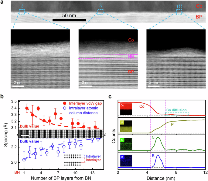
a Low magnification bright-field image of the Co/BN/BP heterostructure’s cross-sectional interface (scale bar 50 nm). Labels i–iii refer to magnified atomic-resolution bright-field images of the denoted regions, showing that the BP vdW structure and stacking is intact over 100’s of nm. b Evolution of the vdW interlayer gap (red) and monolayer thickness (blue), extracted from STEM cross-sections (inset), as a function of distance to the BN/BP interface (in number of BP monolayers). Scale bar: 1.5 nm. The lower inset illustrates our definition of the two plotted distances. c Line cuts of the elemental abundance perpendicular to the Co/BN/BP interface, extracted from electron energy loss spectra (EELS). The four coloured panels are energy dispersive spectrum (EDS) maps for the elements Co, P, N and B.
To further characterize the Co penetration, we did electron energy loss spectroscopy (EELS) along Co/BN/BP cross-sections, and obtained the elemental profiles shown in Fig. 5c. The depth profile of Co shows a penetration depth ~ 5 nm, with an average doping of around 3%. This can be controlled by the initial BN thickness and post-annealing process under high vacuum condition (See Supplementary Table S1 and Supplementary Fig. S9). Although the presence of cluster-free Co-BP is thus consistent with our transport data, it may not be the only possible explanation. The Co diffusion process may inevitably create certain atomic defects in the BN layers and the topmost BP layer, which could also contribute to the TMR switching and requires future experimental and theoretical investigation.
The AHE in p-type BP, the large hysteretic in-plane MR seen in planar transport and spin-valve switching behaviour observed in the MTJs are well-established hallmarks of robust FM order in Co-BP. Its vdW nature and electronic two-dimensionality are decisive in allowing non-detrimental magnetic doping and potentially large FM coupling. The coupled FM and semiconducting functionalities with high charge mobility up to room temperature is distinct from the types of electrical tunability commonly encountered in magnetic systems45 (See the comparison with other magnetic semiconductors in Supplementary Table S2). Given its electronic versatility30, its long spin-diffusion length31, and recent advances in large-scale growth and integration of BP46, our work opens the prospect of employing Co-BP as an active semiconducting FM element in potential spintronics applications without suffering conductivity mismatch problem. This methodology could also be applied beyond BP (Supplementary Fig. S10), thereby expanding the library of low-dimensional magnetic materials. Developing encapsulation techniques to ensure the practical use of our Co-BP devices will be a subject for further investigation in future.