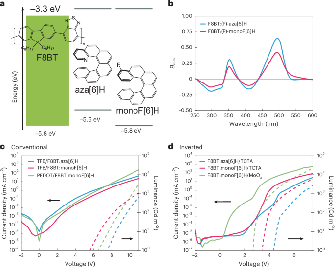
Although aza[6]H has proved to be a useful additive to generate blend polymer films with large chiroptical activity, the optoelectronic performance of poly(9,9-dioctylfluorene-alt-benzothiadiazole) (F8BT):aza[6]H materials are hindered by the shallower highest occupied molecular orbital of aza[6]H (5.4 eV) compared with the highest occupied molecular orbital of F8BT (5.8 eV; Supplementary Fig. 10 and Supplementary Table 1). This results in aza[6]H acting as a hole trap in the blend, which decreases the device performance and limits the type of device configurations that can be used for working OLEDs. To address this issue, we developed fluorine-substituted monoF[6]H, a chiral additive with a deeper highest occupied molecular orbital (5.8 eV) than its aza[6]H counterpart (Supplementary Figs. 1–8), to reduce hole trapping in polymer blends (Fig. 1a). When blended with F8BT at the same concentration (10 wt%) and processing conditions (160 nm thickness), both aza[6]H and monoF[6]H induce a chiral phase in the polymeric film. Annealed blends of (P)-aza[6]H give a dissymmetry factor of lower energy (λ = 491 nm) transition of gabs = 0.65 (CD of 18,200 mdeg), whereas blends of (P)-monoF[6]H have a slightly lower but still substantial dissymmetry factor of gabs = 0.42 (CD of 12,000 mdeg; Fig. 1b and Supplementary Fig. 11). The CD of these films contains negligible contributions from linear dichroism and linear birefringence, with no CD sign inversion on rotation or flipping of the samples (Supplementary Figs. 13 and 14). This was further confirmed by Mueller matrix polarimetry (MMP) data showing that the CD elements m30 and m03 are symmetric whereas circular birefringence elements m21 and m12 are antisymmetric (Supplementary Figs. 15 and 16), which is consistent with prior studies on aza[6]H (ref. 8). This excludes any structural contributions to CPL, with the high chiroptical activity being attributed to the strong excitonic coupling between polymer-chain chromophores21. When optically excited, no change in the emitted CPL handedness is observed for a given enantiomer, regardless of the excitation geometry (Supplementary Figs. 18 and 19).
Conventional and inverted devices were fabricated with the same emissive layer thickness (160 nm). Conventional CP-OLEDs (Fig. 1c) of F8BT:(P)-aza[6]H blends with poly(9,9-dioctylfluorene-alt-N-(4-sec-butylphenyl)-diphenylamine) (TFB) as an additional hole transport layer (HTL) had lower efficiencies and higher turn-on voltages compared with F8BT:(P)-monoF[6]H-based devices (Supplementary Figs. 20 and 21). Furthermore, although the HTL is required to realize working CP-OLEDs for F8BT:(P)-aza[6]H blends, devices using F8BT:(P)-monoF[6]H can be fabricated HTL-free and maintain lower turn-on voltages compared with CP-OLEDs with aza[6]H (Supplementary Table 2). Inverted CP-OLEDs for all conditions (Fig. 1d) show higher device efficiencies compared with the conventional architecture (Supplementary Figs. 22 and 23). Consistent with conventional devices, inverted devices using F8BT:(P)-aza[6]H require (tris(4-carbazoyl-9-ylphenyl)amine) (TCTA) as an HTL, whereas F8BT:(P)-monoF[6]H-based CP-OLEDs can operate without an HTL. Inverted monoF[6]H-based CP-OLEDs demonstrate high efficiencies and, for HTL-free devices, very low efficiency roll-off (Supplementary Fig. 23 and Supplementary Table 2). The superior performance of CP-OLEDs incorporating F8BT:(P)-monoF[6]H confirms that the new chiral additive reduces the trapping caused by aza[6]H.
The lower density of trap states in F8BT:monoF[6]H blends is also supported by hole transport measurements via the space-charge-limited current method (Supplementary Figs. 24 and 25 and Supplementary Table 3). Almost three orders of magnitude difference in the hole mobility was observed in comparing blends of monoF[6]H and aza[6]H, with higher hole trap densities in aza[6]H blends. Mobility measurements of bilayers including an HTL reveal that for aza[6]H blends, the HTL improves hole mobility, whereas for monoF[6]H, it limits the injection of holes, pinning the RZ close to the anode in both cases. No differences in electron transport properties of the two additives were observed, even when measured in bilayers with an electron transport layer (Supplementary Fig. 25b and Supplementary Table 3). These measurements, performed using the same device stack as the respective CP-OLEDs, reveal that (1) in devices (conventional and inverted) with an HTL, the RZ is pinned near the HTL interface and (2) in HTL-free devices, the RZ is located closer to the centre of the stack due to balanced charge carrier injection and transport. This is consistent with the measured efficiency roll-off: efficiency roll-off is minimized in HTL-free devices due to the more balanced charge recombination and reduced quenching (Supplementary Fig. 27). Stability measurements further support this analysis, with conventional and inverted HTL-free devices showing improved stability compared with counterparts with an HTL (Supplementary Fig. 28). Capacitance–voltage (CV) and capacitance–frequency (CF) measurements indicate that devices with HTLs suffer from charge accumulation and capacitance build-up due to the unbalanced charge carrier mobility and the pinned RZ close to the HTL. Specifically, HTL-free devices feature a sharp drop in capacitance after turning on in CV measurements, whereas devices with an HTL feature a capacitance build-up (Supplementary Fig. 29). CF measurements, carried out after device turn on, also feature a higher capacitance at low frequencies in HTL-free devices (Supplementary Fig. 30). Both these characterizations demonstrate charge accumulation and capacitance build-up due to unbalanced charge carrier mobility and support the location of the RZ near the interface with the HTL.
Enabled by the discovery of a chiral polymeric material with improved hole mobility, it was found that the handedness of CP-EL could be controlled through the use of conventional and inverted F8BT:(P)-monoF[6]H CP-OLEDs, with or without HTLs (Fig. 2). Without an HTL (Fig. 2a,b), the RZ of OLEDs using F8BT:(P)-monoF[6]H is in the middle of the active layer. The measured CP-EL retains the same handedness irrespective of the device architecture (preferentially left handed for the P enantiomer of monoF[6]H, gEL CONV = +0.10 and gEL INV = +0.13). This is the same handedness as optically pumped CP photoluminescence (gPL = +0.24). Together with the fact that the handedness of CPL cannot be inverted by changing the current flow direction, this suggests NCPE for F8BT:(P)-monoF[6]H CP-OLEDs without an HTL (Supplementary Figs. 33 and 35). Consistent with this assignment, measurements on semitransparent devices show the same magnitude and handedness of CP-EL regardless of the measurement direction: gEL,ITO = +0.12 and gEL,Al = +0.10 in the case of conventional semitransparent devices (Supplementary Fig. 33) and gEL,ITO = +0.12 and gEL,Au = +0.10 for inverted semitransparent devices (Supplementary Fig. 35). This is also consistent with the handedness of CPL emitted from thin films on optical excitation at different geometries. NCPE restricts the total gEL of the device: the back electrode changes the phase of polarization, reversing its handedness and partially cancelling CPL emitted towards the transparent electrode (gEL gPL). The small differences in gEL between conventional and inverted devices can be attributed to optical losses due to the attenuation of CPL propagating inside the device (Supplementary Note 3). For the same reason, the sum of gEL obtained from semitransparent devices does not match the gEL measured in devices with highly reflective electrodes.
Fig. 2: Electrical control of CP-EL.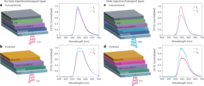
a, Device architecture (ITO/PEDOT:PSS/F8BT:monoF[6]H/TPBi/Ca/Al) and CP-EL characteristic of conventional HTL-free CP-OLEDs. b, Device architecture (ITO/ZnO/PEIE/F8BT:monoF[6]H/MoOx/Au) and CP-EL characteristic of HTL-free inverted CP-OLEDs. c, Device architecture (ITO/PEDOT:PSS/TFB/F8BT:monoF[6]H/TPBi/Ca/Al) and CP-EL characteristics of conventional devices, with TFB as the HTL d, Device architecture (ITO/ZnO/PEIE/F8BT:monoF[6]H/TCTA/MoOx/Au) and CP-EL characteristics of conventional devices, with TCTA as the HTL. The thickness of all emissive layers is 160 nm. IL, intensity of left-handed (LH) light; IR, intensity of right-handed (RH) light.
In conventional devices with an HTL, the handedness of CP-EL inverts compared with devices without the HTL (Fig. 2c) and right-handed emission is preferred for the P enantiomer of monoF[6]H (gEL CONV = –0.40). By contrast, left-handed emission is still preferred for the P enantiomer of monoF[6]H when used in inverted devices with an HTL (gEL INV = +0.38; Fig. 2d). As such, the handedness of CPL is clearly inverted by changing the current flow direction for F8BT:(P)-monoF[6]H CP-OLEDs with an HTL, suggesting ACPE. Measurements using semitransparent devices showed that conventional devices with a TFB HTL gave opposite-handed CP-EL as a function of emission direction (gEL,ITO = −0.22 and gEL,Al = +0.23; Supplementary Fig. 34). Inverting the device structure when using TCTA as an HTL also results in opposite-handed CP-EL, but with the absolute handedness inverted relative to conventional devices with an HTL (gEL,ITO = 0.33 and gEL,Au = −0.27; Supplementary Fig. 36). The emission of CPL is non-reciprocal: CPL emitted towards the top electrode inverts handedness, partially combining with CPL emitted towards the ITO and increasing the measured gEL. This overcomes the theoretical limit of devices with only NCPE (gEL > gPL). Supplementary Fig. 37 evaluates the impact of HTL thickness in inverted devices, where the HTL is evaporated rather than solution processed. It is clear that the HTL thickness does not impact |gEL|, but it does impact the EL lineshape due to cavity effects22.
In summary, the electrical control of CP-EL handedness is observed simply through the addition or omission of an HTL within the device stack. Devices without an HTL show NCPE, whereas devices with an HTL show APCE. In all the devices (that is, with ACPE and NCPE), gEL is independent of current density, which is consistent with previous results in chiral polymer blends (Supplementary Fig. 38). Although the absolute gEL values achieved in this work are not the highest reported so far, they remain among the highest in the field. This impressive performance is accompanied by the first demonstration of electrical control over the emission mechanism (Supplementary Table 5), achieved through careful material and device design.