VHS-driven photodetection mechanism
RVS system consists of planar V-atom kagome networks, intervening Sb honeycomb layers, and triangular Rb-ion planes separating the V-Sb slabs, as illustrated in Fig. 1a. RVS undergoes a CDW phase transition at TCDW ( ~ 102 K)33, which is accompanied by substantial electronic band structure reconstruction, building upon prior research on kagome systems34. Figure 1b, c illustrate three key electronic band features of an ideal kagome lattice at the normal state: (i) Dirac cones at the K point, (ii) VHS at the M point, and (iii) momentum-space flat bands. Figure 1d, e illustrate the unit cell configurations of RVS in the normal state and CDW state, respectively. The CDW transition in RVS, within a simple planar case, yields a 2 × 2 long-range charge ordering pattern, causing an Inverse Star of David (ISD) structure in the plane characterized by a doubling of the primitive cell22. Figure 1f presents the electronic band structure at the normal state computed along the Γ-K-M-Γ symmetry line, revealing the predicted pair of VHSs flanking EF near the M point (designated as VHS1 and VHS2 in Fig. 1f). The VHS1 and VHS2 near the EF exhibit complementary dispersion relations—electron-like along Γ-M and hole-like along M-K. This generates a divergent DOS, as confirmed by our calculations. Utilizing the divergent DOS at VHS, we demonstrate photoelectric conversion across both normal and CDW phases (Fig. 1g). Notably, upon entering the CDW state (T < TCDW), the VHS near the M point progressively shifts away from the EF (Fig. S7). This unique VHS redistribution provides a well-defined mechanism for photoresponse enhancement of non-equilibrium carrier transition probabilities (Fig. 1g), which is systematically analyzed in subsequent sections.
Fig. 1: Phase transition in RVS and the resultant enhancement of photoelectric conversion efficiency.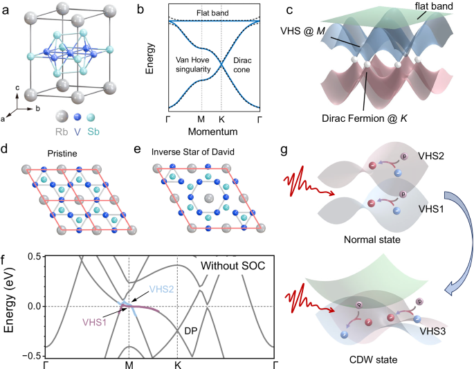
a Unit cell of RVS. b,c 2D and 3D schematic representations of kagome materials band structure characteristics. d,e Top-view crystal structures of RVS in normal state and CDW state, respectively. The CDW state exhibits a well-defined 2×2 ISD superlattice configuration, with the crystallographic unit cell boundaries clearly demarcated by pink guidelines. f Calculated band structure including spin-orbit coupling along the Γ- M- K- Γ direction. g VHS- driven photoelectric conversion mechanism at normal state and CDW state.
Singular electronic band behavior in RbV₃Sb₅
To elucidate the photoelectric detection mechanisms in RVS, we perform density functional theory (DFT) calculations and angle-resolved photoemission spectroscopy (ARPES) observations (Methods). Our comparative analysis between theoretical and experimental results elucidate the emergence of VHS3 in the CDW phase. The exceptional crystalline quality of the material (detailed in Supplementary Note 1) ensures experimental reproducibility. Figure 2a presents the temperature-dependent in-plane resistivity of RVS, revealing a distinct anomaly at approximately 102 K. This feature is characteristic of a CDW phase transition, consistent with established observations in correlated electron systems33. As established in prior investigations35, the TCDW exhibits pronounced thickness dependence in AVS materials. Our systematic study employs an approximately 140 nm-thick sample—a dimensionality carefully selected to maintain bulk-like electronic properties while avoiding the 3D-to-2D crossover regime. Additionally, our results reveal that the pristine phase exhibits marked structural instability. Phonon spectrum, performed on a 3 × 3 × 1 supercell, reveals significant phonon mode softening around the M and L points of the Brillouin zone (BZ) boundary in the RVS phonon dispersion (Fig. 2b), unambiguously indicating inherent structural instability in the pristine phase36,37. This lattice dynamical instability serves as the driving mechanism for the CDW phase transition.
Fig. 2: Experimental evidence of CDW formation in RVS and VHS signature from electronic structure analysis.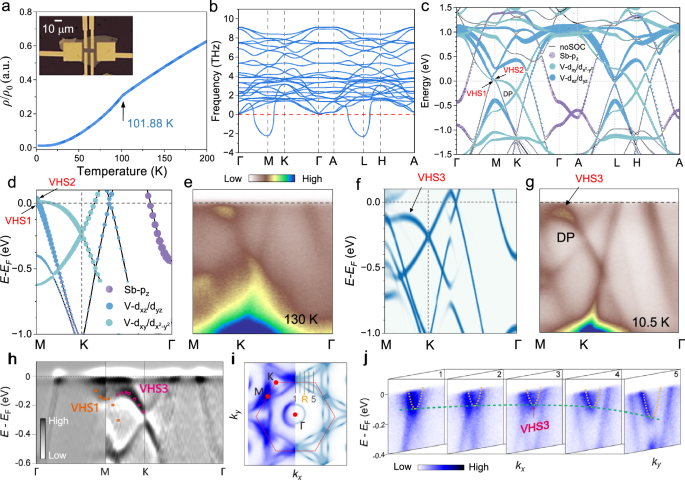
a Resistivity-temperature curve showing a distinct anomaly in the 90–102 K range, signaling the phase transition in the material. The inset is the Hall bar device used for resistivity characterization in RVS. b Calculated phonon spectrum for the normal phase of RVS. c Band structure of RVS in the normal phase projected onto the V-d and Sb-p orbitals. The gray lines represent the band structure without SOC the lines with circles represent the band structure with SOC. The size of the circles reflects the proportion of orbital components. d Calculated band structure for the normal state, with SOC, along the M-K-Γ direction. The red arrows indicate VHS1 and VHS2. e ARPES spectra at 130 K (above TCDW) along the M-K-Γ direction. f Calculated band structure for the ISD CDW state along the M-K-Γ direction, and g ARPES spectra of the CDW phase taken along the same direction at 10.5 K (below TCDW). h Second derivative spectrum along the high-symmetry path M-K-Γ at 10.5 K (below TCDW). The dotted line enhances the visibility of the energy bands near the M point, clearly revealing the band structure around VHS1 and VHS3. i Experimental and theoretical Fermi surface comparison. Orange marker indicate the R direction. j ARPES spectra from the momentum-space trajectories (cuts 1–5) in Fig. 2i as indicated by gray lines. The yellow dashed lines highlight the electron-like band, while the green dashed line indicates the hole-like band. The arrow in cut 3 indicate the appearance of VHS3.
By combining theoretical and experimental results, we focus our investigation on a unique feature in the electronic band structure: VHS. Figure 2c displays the DFT-derived electronic structure of RVS, showing orbital-projected (V 3d, Sb 5p) band dispersions in the primitive lattice with (colored) and without (gray) spin-orbit coupling (SOC). Three key characteristics are observed: (i) a dispersionless band across nearly the whole BZ at \(1.00\pm 0.05\) eV above EF, (ii) Γ-centered electron pockets and Dirac cones dominated by V 3d states near the K point, and (iii) multiple VHSs near M (black arrows) arising from V 3d-Sb 5p hybridization. The VHS1 and VHS2 are particularly significant, positioned within 10 meV of EF and exhibiting complementary dispersion relations—electron-like along Γ-M and hole-like along M-K. This generates a divergent DOS, as confirmed by our calculations.
For low-energy photon detection, we systematically investigate the VHS near the EF in the normal phase and CDW phase. Calculated and ARPES-measured band structures along the high-symmetry paths demonstrate exceptional consistency (Fig. 2d, e). Despite thermal broadening effects at elevated temperatures, we identify two pivotal phenomena: (i) a well-defined hole-like band dispersion along the K-M high-symmetry path, and (ii) the dominant contribution of V d-orbital states to the formation of the VHS. VHS1 manifests hallmark VHS characteristics, exhibiting contrasting dispersion relations along the M–Γ (upward) and M–K (downward) directions. This characteristic leads to a pronounced DOS peak near EF. Figure 2f, g respectively show the theoretically predicted band structure of the ISD state and corresponding ARPES measurements (TCDW). The strongly dispersive band along the K-M undergoes a significant downward shift ( ~ 0.14 eV at the M point) relative to the normal state, thereby forming a distinct VHS1.
Intriguingly, near the midpoint of the M-K trajectory, the V d-orbital hybridization shows discontinuity and a CDW gap is open. Correspondingly, the part of the band below the EF also undergoes a downward shift, moving entirely below EF. This is clearly captured at ~0.09 eV below EF in the low-temperature experimental results. More intriguingly, a new VHS configuration emerges here, characterized by a hole-like pocket along the M-K direction and an electron-like pocket in the perpendicular direction. A detailed analysis of the band structure at TCDW (Fig. 2h, second-derivative plot along the Γ-K-M-Γ) reveals a new VHS3 ( ~ 0.09 eV below EF) near the M-K midpoint (pink marker).
To further verify the characteristics and momentum location of VHS3, Fig. 2i demonstrates exceptional consistency between cryogenic temperature DFT calculations and cryogenic temperature ARPES-derived Fermi surfaces, featuring spectral cuts (1-5) at discrete kx positions along the K-M-K path. A systematic examination through ARPES cuts (Fig. 2i,j) unambiguously establishes the saddle-point character of VHS3.The data show that the band maintains an electron-like dispersion along ky (yellow dashes) at all kx positions, while hole-band features (green dashes) with varying kx, which confirms the saddle point. The temperature evolution of the electronic band structure along the K-M-Γ path is annotated in Fig. S7. The downward shift of the V d bands and the formation of new VHS lead to a high DOS crossing the EF, thus leading to electronic structure instability. The calculated DOS exhibits robust agreement with the experimental findings. In both the normal state and CDW state, the DOS exhibits a peak at the saddle point due to the accumulation of occupied states where the electronic band dispersion exhibits a vanishing group velocity (detailed in Supplementary Note 4). Additionally, while the in-plane orbital-dominated Dirac bands near K remain essentially unaffected, the Γ-point electron pocket—composed primarily of out-of-plane \({p}_{z}\) orbitals—exhibits a pronounced energy shift. This collective behavior provides definitive evidence for a temperature-driven phase transition with Fermi surface reconstruction. These findings demonstrate that VHSs emerge from band structure extrema and saddle points occur at strategic locations that fundamentally govern optoelectronic response.
VHS-governed exotic phenomena through direct configurations
Our analysis reveals that RVS undergoes significant topological modifications near its TCDW, manifesting as band structure evolution, Fermi surface reconstruction, and pronounced VHS rearrangements. These emergent properties create unprecedented opportunities for low-energy photon detection. Our work demonstrates—for the first time—the direct utilization of kagome-derived topological states for photodetection. We now present the remarkably promising experimental results in photodetection.
We develop the structure of the kagome-metal-based photodetector (Fig. 3a), comprising a bowtie antenna-which serves as electrodes and features a left-right symmetric optical field efficiently coupling photon energy into the channel-and the kagome material RVS38. The RVS channel layer is prepared by mechanical exfoliation, and the device is meticulously patterned into a planar configuration. (further details are provided in the Methods). Complete finite-difference time-domain (FDTD) simulation details are provided in Supplementary Note 5.
Fig. 3: Experimental direct detection of the photocurrent response in a kagome material-based detector.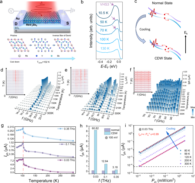
a Schematic diagram of the optoelectronic device based on kagome metal is presented, with metal electrodes labeled as source and drain. The photoresponse changes induced by temperature variations are extracted from the source and drain terminals. b Corresponding EDC at the M-point reveals the temperature-dependent evolution of peak shifting behavior. c Mechanism of photoinduced response in kagome metals in normal and CDW state. d–f Temperature-dependent photoresponse current across frequency ranges of 20–40 GHz, 80–100 GHz, and 330–355 GHz. New VHS formation and original VHS redistribution below TCDW enhance photoresponse. The insets show response maps at the corresponding frequencies and temperatures, where the photoresponse intensity gradually increases from light blue to red. g Measured the temperature-dependent photoresponse current at frequencies of 0.03, 0.1, and 0.35 THz. Upon cooling, the emergence of the VHS leads to an anomalous enhancement of the THz photoresponse. The inset illustrates the top view of the lattice structure before and after the phase transition temperature. h Comparison of photocurrent intensity between the normal and CDW state. i Power-dependent photoresponse of devices across five temperature points (77–300 K) at optical excitation densities spanning 0.06–2.5 mW/cm².
The energy distribution curves (EDCs) extracted near the EF region (Fig. 3b) demonstrate the dynamic evolution of the RVS system’s band structure with decreasing temperature (from 130 to 10.5 K). In the normal state (T > TCDW), both VHS1 and VHS2 at the M-point maintain their positions and exhibit minimal temperature dependence. In the CDW state (T < TCDW), the electronic states near the M-point undergo a progressive shift toward higher binding energies with decreasing temperature (further details illustrated in Fig. S7). In kagome systems exhibiting Fermi surface nesting characteristics, these observations provide key insights into the microscopic physical mechanisms underlying electronic instabilities. The VHS exhibits intrinsic electronic instability. Fermi surface nesting facilitates enhanced electron scattering along its characteristic wavevector. Simultaneously, the emergence of a new VHS3 feature leads to a significant amplification of the DOS at the EF33. The strongly enhanced DOS at these singularities creates ideal conditions for low-energy photon detection. Figure 3c elucidates the microscopic mechanism governing the enhanced photoresponse, showing that the VHS-induced DOS peak increases the number of available initial states for the optical transition.
Our full-spectrum analysis reveals distinct temperature-dependent photoresponse characteristics of the photodetector across three key THz bands (0.02–0.04, 0.08–0.1, and 0.33–0.355 THz) at 0 mV bias. Figure 3d–f demonstrate that the photoresponse intensity, color-graded from dark to light blue (strongest to weakest), consistently peaks at TCDW ~ 102 K in all frequency ranges. The top-view schematics (Fig. 3d–f, insets) spatially resolve these response maxima. As the photocurrent intensity exhibits a positive correlation with the DOS, we derive the quantitative relationship expressed in Eq. 1.
$$J (\omega )\propto e \cdot D\left(E\right) \cdot {\left|\left\langle {f}\left|{\hat{H}}_{{int}}\right|{i}\right\rangle \right|}^{2} \cdot \hslash \omega \cdot \Phi \left(\omega \right)$$
(1)
where \(J\left(\omega \right)\) denotes photocurrent density, e represents electron charge, D(E) corresponds to the electronic DOS, \(\left\langle {f|}{\hat{H}}_{int}{|i}\right\rangle\) describes transition matrix element incorporating initial state, final state, and perturbation Hamiltonian, \(\hslash \omega\) is incident photon energy, \(\Phi (\omega )\) describes incident photon flux. As clearly demonstrated by the simplified Eq. 1, the photocurrent density is directly influenced by the electronic DOS39. In the normal state of kagome metal RVS, two VHSs exist near the EF at the high-symmetry M-point. CDW phase transition renormalizes the band structure and new VHS emerges. Since the electronic DOS exhibits logarithmic divergence near VHS, the phase transition therefore enhances the photocurrent density \(J\left(\omega \right)\) through increased D(E).
Under an applied bias of 100 mV, we systematically measured the temperature-dependent photoresponse of the RVS-based detector at 0.03, 0.09, and 0.35 THz (Fig. 3g). Experimental results indicate that at TCDW ( ~ 102 K), the device’s photoresponse exhibits significant nonlinear enhancement. Notably, applying a 100 mV bias maintains the peak frequency while significantly enhancing the photocurrent intensity (full spectral scans available in Supplementary Note 8). This enhancement mechanism arises from bias-excited electronic transitions between VHS.
Figure 3h compares the photoresponse enhancement between the normal and CDW phases at a 100 mV bias, revealing frequency-dependent amplification factors of 60.82 × (0.03 THz); 12.64 × (0.1 THz); and 3.18 × (0.35 THz). This enhancement aligns with theoretical predictions: the phase transition redistributes VHS and modifies the electronic DOS near critical points, thereby amplifying interband transitions. Our results establish kagome materials as a platform for frequency-selective photoresponses through many-body correlations.
The second-order photocurrent (Iph) scaled linearly with the incident electric field power (Pin) across temperatures (77–300 K), as shown in Fig. 3i. The photodetector exhibits ideal linearity over more than two orders of magnitude in Pin and the data are well fitted with a simple power law (\({I}_{{{\rm{ph}}}}\propto {P}_{{{\rm{in}}}}^{\alpha },\)α\(=0.99\pm 0.005\)) at all measured temperatures40. This temperature-independent nonlinearity is a direct manifestation of the RVS system’s singular electronic structure, where VHS-derived DOS enhances multiphoton processes. Our results establish kagome materials as a unique platform for wide-temperature-range nonlinear photonics.
Noise is a critical parameter influencing the performance of optoelectronic devices. Once the temperature is below TCDW, the electronic noise spectral density shows a dramatic reduction by over two orders of magnitude (from 3.8 × 10⁻²³ A/Hz2 to 1.38 × 10⁻²⁵ A/Hz2). The system exhibits enhanced stability upon entering the CDW state, with significantly reduced random carrier scattering events. The Noise Equivalent Power (NEP) is a critical parameter. Across the entire modulation frequency range, the device achieves an average NEP of approximately 20 pW/ Hz1/2. Operating at 0.1 THz, our device demonstrates ultrafast response characteristics with 580 ns rise time and 520 ns fall time, which is several orders of magnitude faster than other thermoelectric detectors (such as ≈ 170 µs of tellurium nanowire photodetector41). (see details in Fig. S12)
VHS-driven heterodyne mixing from millimeter wave to THz band
Based on the unique VHS properties as well as band-renormalization of kagome-metals, we further investigate the potential of heterodyne RF detection. In our measurements (details can be found in Methods), the fabricated kagome material-based mixer serves as a frequency conversion device in the circuit (Fig. 4a), which constitutes a critical component in modern RF communication systems42,43.
Fig. 4: Heterodyne detection platform of the kagome material-based mixer operating at different temperature.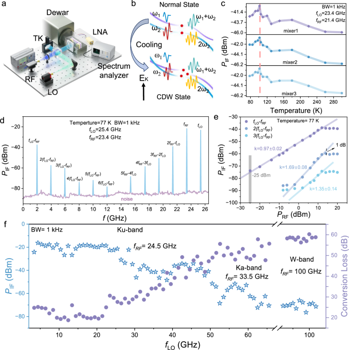
a Temperature-adjustable heterodyne detection platform with full compatibility for mixers. The radio frequency (fRF) and local oscillator (fLO) signals are coupled spatially into the mixer, producing an intermediate frequency signal (fIF = |fRF – fLO | ) that is amplified and analyzed with a high-resolution spectrum analyzer. b Chematic diagram of the frequency conversion mechanism in a kagome material-based mixer for heterodyne detection. c The fIF signal is characterized using a fLO (23.4 GHz) and a fRF (25.4 GHz), under varying temperature conditions. A spectrum analyzer recordes the fIF signals at each temperature condition, with three separate mixers being tested and analyzed to ensure measurement reliability. d Resulting mixed spectrum is recorded using a spectrum analyzer, with each peak appropriately labeled when fLO is set to 23.4 GHz and fRF is 25.4 GHz (in CDW state). e Relationship between the down-converted fIF output power and the input RF power at different fRF power levels is analyzed. The solid line represents the linear fit of the measured values. The 1 dB compression point is marked with a black arrow. f The fIF output and conversion loss demonstrate a frequency-dependent relationship governed by the fLO. The fRF is tuned to cover the Ku, Ka, and W bands.
The heterodyne THz detection system, governed by novel physical mechanisms, achieves broadband operation and high detection sensitivity across phase transitions. The schematic illustration of the mixing process under optical beating within two different frequencies in kagome-based materials is presented in Fig. 4b. The kagome material-based mixer generates distinctive heterodyne signals through coupling of the local oscillator (fLO) and radio frequency (fRF) inputs, yielding an intermediate-frequency beat signal VIF described by:
$${V}_{{IF}}\left(t\right)={L}_{0}\left(t\right){R}_{{THz}}\left(t\right)=\frac{{L}_{o}{R}_{{TH}z}}{2}\left[\cos \left(\omega -{\omega }_{{THz}}\right)t+\cos \left(\omega+{\omega }_{{TH}z}\right)t\right]$$
(2)
where \({V}_{{IF}}\left(t\right)\) represents the intermediate frequency output signal, \({L}_{0}\left(t\right)\) represents the local oscillator signal, \({R}_{{TH}z}\left(t\right)\) represents the radio frequency signal44.
First, we demonstrate harmonic mixing in a kagome material-based mixer under collimated 6.5 GHz excitation. Through spectrum analysis, the first, second, and third harmonic comb lines are clearly resolved, with the harmonic signals exhibiting robust power dependence. Notably, the generated frequency comb also serves as a tunable local oscillator (fLO), enabling versatile heterodyne mixing. The measured fIF adheres precisely to the expected relationship: fIF = fRF – n fLO (n ∈ ℕ+) (Figure S14).
Through temperature-dependent measurements, we implement heterodyne mixing techniques in kagome-material-based mixers to systematically investigate their potential for modern communication technologies. Figure 4c demonstrates the temperature evolution of fIF signal arising from the distinctive VHS inherent to kagome systems. To ensure reliable characterization of mixing dynamics within the spectrum analyzer’s bandwidth constraints, we implement a heterodyne scheme using 22.4 GHz (fLO) and 23.4 GHz (fRF) signals. Control experiments with three independent mixers confirmed the reproducibility of our observations. Notably, we observe a pronounced enhancement in fIF signal intensity as the temperature decreased from 300 K to below TCDW. This anomalous behavior originates from temperature-induced modifications in the electronic band structure: (i) the emergence and upward energy shift of a VHS at the M-point, and (ii) the formation of a secondary VHS at the R-point below TCDW. The cooperative migration of these singularities enhances electronic transitions, resulting in the observed macroscopic amplification of the fIF signal.
Kagome systems exhibit exceptional promise for self-mixing applications as noted above. Building on this foundation, we observe broadband multi-wave-mixing in nonlinear kagome systems. Figure 4d demonstrates the characteristic signatures of subharmonic N-wave mixing (WM) (fLO is 23.4 GHz, fRF is 25.4 GHz and fIF signal is precisely captured by the spectrum analyzer)45. These peaks include three types of spectra: the two fundamental signals (ω₁ = 2πfLO, ω₂ = 2πfRF), the fIF signal (fIF = fRF – fLO), their higher-order modes, and the WM components (n fLO ± m fRF, where n, m = 1, 2, 3…). The highest observed components reach up to 5 (fRF – fLO) and 6 fLO – 5fRF. These results indicate that, due to the material’s highly complex Fermi surface and exotic electronic behavior below TCDW, a frequency comb-like heterodyne mixing effect can be generated, with higher-order components extending up to the fifth order.
To further investigate the dynamic range of the kagome material-based mixer, the relationship between the fIF signals of different harmonic mixing orders and the incident power (PLO and PRF) is shown in Fig. 4e. The relationship follows the power law, \({P}_{{{\rm{out}}}}=\alpha {P}_{{{\rm{in}}}}\) (where Pin = PLO), and the solid line represents the slope of the output power measured in the experiment. Notably, even when the fRF signal is set to its lower limit (PRF = − 25 dBm, PLO = 14.8 dBm), the fIF signals at (fRF − fLO) and (2 fLO − fRF) remain clearly detectable. This indicates that the minimum power excitation threshold of the mixer can be less than -25 dBm, demonstrating the potential of kagome materials for precise carrier frequency information acquisition.
By harnessing the exotic electronic properties of kagome material, we demonstrate the mixing range to the THz band for modern RF communication systems. The fLO is increased to above 100 GHz, approaching the electrical oscillation limit of micron-scale devices. Simultaneously, the fRF is tuned across a range from the Ku and Ka bands to the W band, as shown in Fig. 4f. This shows that the kagome-based device demonstrates intrinsic frequency-agile capture capability, operating across a very wideband range of 1–100 GHz. The conversion loss (CL) increases monotonically with the fLO, escalating from 20.1 ± 0.2 dB to 57.5 ± 0.2 dB at 100 GHz. This performance highlights the device’s promising applicability in next-generation wireless communication systems.
The frequency CL, defined as one of the key metrics for mixers46, is expressed as:
$${CL}=\frac{{P}_{{in}}}{{P}_{{out}}}=10\cdot \log \left(\frac{30{P}_{{RF}}}{{P}_{{IF}}}\cdot \frac{{S}_{\lambda }}{S}\right)$$
(3)
where, 30 represents the gain coefficient of the LNA, \({S}_{\lambda }={\lambda }^{2}/4\pi\) represents the diffraction-limited area within the incident wavelength; S represents the area of the waveguide flare. The CL of the mixer near 100 GHz is 57.5 ± 2 dB, while the CL in the RF band is 20 ± 2 dB.