Overview
Our device is a JJ electrostatically defined in MATBG, with a twist angle of 1.06∘ ± 0.04∘, also studied in reference18 (Fig. 1a). The global carrier density n, tuned by the back gate, is set to n = −1.73 × 10⁻¹² cm−2, at which the bulk has its highest critical current, 250 nA (See SI). Two layers of top gates, separated by a layer of Al2O3, tune the local density in the central region, allowing us to fine-tune the details of the junction.
Fig. 1: Device response to AC and DC biases.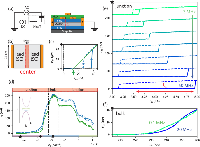
a Schematics of the device. The device is depicted by a cross section schematics. The vertical red dashed lines represent the central (C) region highlighted in (b). b Top-view simplified schematics with the gold contacts on the side, connected by a stripe of magic-angle twisted bilayer graphene (MATBG). The central region, of length 100 nm, is highlighted. The leads are superconducting (SC). c I/V characteristic of the junction at a density of −2.8 × 1012 cm−2. In blue, solid line, a trace for increasing DC bias is shown. The dashed line represents the trace for decreasing bias. The green line is an extrapolation of the resistive part of the characteristic at 0 voltage. The green arrow highlights what is defined as excess current. d Switching (blue), retrapping (blue, dashed) and excess (green) currents as a function of density in the central region. The colors on the x-axis correspond to the filling of the band structure schematics shown in the inset. The upper part indicates whether the I/V characteristic shows a junction-like or bulk superconductor-like behavior. The black star, circle and square indicate, respectively, the densities at which is taken the data shown in (e, c, f). e I/V traces of the junction for AC bias of increasing frequency and fixed amplitude (red arrow) as a function of DC bias (horizontal axis). Solid lines show positive bias directions while dashed ones show negative directions. Curves are offset vertically for readability. f I/V traces at bias AC amplitude 1.4 nA and frequencies of 0.1 MHz and 20 MHz when the sample is tuned to all-bulk configuration see panel (d).
For each value of electron density in the central region (Fig. 1b) we analyze the current-voltage (I/V) characteristic. For densities in the central region close to nj = −2 we observe a gradual onset of resistance above a critical current value, consistent with bulk superconductivity (see also discussion of Fig. 1f below). For all other densities, we universally observe a hysteretic I/V trace with two characteristic voltage jumps ΔV, as shown in Fig. 1c. The two jumps correspond to switching from the superconducting to the resistive state (increasing current bias, blue line) and retrapping back (decreasing current bias, blue dashed). Together with Shapiro step measurements18 this indicates the formation of a weak superconducting link between the left and right parts of the device, where the weak link region can switch between resistive and superconducting states. From the band structure of MATBG2 (see inset of Fig. 1(d), for a schematic), the weak link region is expected to be metallic except for a narrow range of voltages placing the chemical potential into the gap between the flat and dispersive bands. Such assessment is consistent with the observation of a positive excess current, Iex,24,25 in the resistive state of a large portion of the phase diagram (green curve in Fig. 1d). In analogy to conventional superconductors17, the dynamic response of such metallic weak links should give access to the dynamics of the electronic quasiparticles and the superconducting condensate in MATBG. We probe the dynamics of our weak links by adding a small AC current component to the DC current flowing through the junction. Sweeping the frequency across three orders of magnitude (0.1–100 MHz), we focus on the changes in the I/V characteristics, as shown in Fig. 1e. At low frequencies, the AC drive brings the two hysteresis branches closer together, which can be understood as follows. The abrupt character of switching and retrapping with DC bias suggests that the junction will undergo a change whenever the total current IDC + IRF(t) reaches the critical value for switching (Isw) or retrapping (\({I}_{{{\rm{re}}}}\)). Consequently, one expects the switching to occur prematurely at Isw − IRF, and the retrapping to occur at a higher DC bias, \({I}_{{{\rm{re}}}}+{I}_{RF}\), reducing the size of the hysteresis loop.
For increasing frequency, the effect of AC bias gradually disappears (Fig. 1e), with a different rate for switching and retrapping. This indicates that both processes, in fact, do not occur instantaneously and are characterized each by a certain rate, which we denote as Γre and Γsw. We note that under switching (retrapping) rate we mean the characteristic scale for the switching (retrapping) current dependence on AC bias frequency, with a precise definition of that scale given below. At highest frequencies, the AC drive effect is absent, indicating that neither switching nor retrapping processes are fast enough to occur over one AC drive period. The switching and retrapping rates that can be extracted from Fig. 1e reflect the properties of superconducting MATBG. We now turn to their physical interpretation.
Modeling the weak link
We can first rule out switching and retrapping driven only by the dynamics of the superconducting phase difference across the junction, exemplified by, e.g., the Resistively and Capacitively Shunted Junction (RCSJ) model24. In that case, the characteristic frequency is fixed by the Josephson relation to 2eΔV/ℏ. For our weak links it is of the order of 10 GHz, several orders of magnitude larger than the frequencies used in our experiments. The RCSJ model also predicts the switching rate to be smaller than the retrapping one, inconsistent with experimental observations (see additional discussion in Supplementary Information). We therefore conclude that our experimental observations require a mechanism beyond the RCSJ model to explain the switching and retrapping charateristics.
Such an alternative mechanism, for both the retrapping and the hysteresis in metallic weak links is the heating of the electrons in the junction, followed by their thermalization17,26. In this case the retrapping branch at I Isw is characterized by a higher temperature than the switching one due to the Joule heating in the resistive state (Fig. 2a, b). This overheating reduces the weak link critical current for the retrapping branch, leading to a hysteresis. Most importantly, retrapping back into the superconducting state requires the electronic temperature to equilibrate to base temperature, a process, depicted in Fig. 2c, that has been directly demonstrated in superconductor-normal metal-superconductor junctions17.
Fig. 2: Model for the switching and retrapping mechanisms.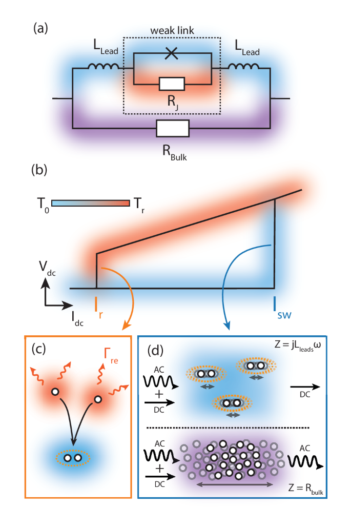
a Equivalent scheme of the MATBG junction for densities inside the lower flat band: the weak-link region modelled as a resistively shunted junction is coupled in series with the kinetic inductance of the leads. The superconducting regions (blue and red) are further shunted by normal regions (purple). b Illustration of switching and retrapping mechanism and hysteresis origin in MATBG junctions. \({I}_{{{\rm{re}}}}\) and Isw represent, respectively, the retrapping and switching currents. The retrapping branch of IV characteristic (red) is characterized by an increased electronic temperature Tr due to Joule heating, suppressing the critical current. Retrapping into the superconducting state requires cooling the electrons (c) to base temperature characterized by a rate dependent on electronic cooling power Gth. Switching rate (blue), on the other hand, is only limited by the shunting kinetic inductance of the bulk MATBG (a, d). c Electronic thermal relaxation in MATBG occurs via coupling to acoustic phonons. Two electronic quasiparticles in the junction release their thermal energy to the phonon bath and become cold enough to mediate Josephson coupling. This coupling is represented by an orange dashed line. Γre represents the thermalization rate. d Due to their inertia, Cooper pairs in a thin superconductor (blue region) prevent the transmission of RF signals at high frequencies. Instead, the AC current at frequencies above \({\omega }_{L}=\frac{{R}_{bulk}}{{L}_{{{\rm{leads}}}}}\) is rerouted through non-superconducting regions of the sample (purple region) and does not affect the junction. Z represents the impedance seen by the signal, Rbulk the resistance of the bulk and Lleads the inductance of the leads.
While there are several mechanisms for energy dissipation in graphene, at low temperatures the dominant one is the coupling between electrons and acoustic phonons. In particular, thermalization can occur via diffusion of hot electrons into the leads, emission of blackbody photons or interaction of electrons with acoustic phonons (as the optical ones are frozen out)27. The first mechanism is suppressed by the presence of a superconducting gap28 in the leads in our case, while the second one has been estimated to be negligible in MATBG29,30. This suggests that the dominant heat loss mechanism is via coupling to phonons, in agreement with conventional SNS junctions17,26.
The above mechanism on its own, however, still implies that switching occurs with the Josephson rate 2eΔV/ℏ, which is inconsistent with our observations, as detailed above. To understand the switching dynamics in our devices we now turn to the case without a central gate voltage, i.e., where the sample is homogeneously superconducting at the optimal density. We observe a frequency-dependent IV characteristic (Fig. 1f), despite the absence of a weak link. Note that there is no hysteresis, ruling out overheating as its origin.
In addition to these observations, it has been shown that a supercurrent can flow in MATBG in narrow superconducting paths separated by normal regions31. The normal region thus forms a resistive shunt Rbulk coupled in parallel to the superconducting regions (purple shaded path in Fig. 2a). At a non-zero frequency ω, the superfluid impedance is purely inductive due to the inertia of the Cooper pairs (blue shaded mechanism in Fig. 2d) and given by Zsc = jωLkin, with the kinetic inductance \({L}_{{{\rm{kin}}}}\propto \frac{{m}^{*}}{{n}_{{{\rm{s}}}}{e}^{2}}\), where m* is the effective mass, e the electron charge, and ns is the superfluid density. At frequencies larger than \(\frac{{R}_{{{\rm{bulk}}}}}{{L}_{{{\rm{kin}}}}}\), the impedance of the superconducting branch becomes higher than the resistance of the normal bulk and the AC current flows through the non-superconducting regions (purple shaded mechanism in Fig. 2d). Intriguingly, Lkin in MATBG is expected to be large19 due to two unique properties: extremely low electron densities, and high effective mass1. This explains our observation of a rather low characteristic switching rate in Fig. 1f. The same mechanism applies for MATBG weak links – the kinetic inductance of bulk MATBG is then coupled in series to the junction (Fig. 2a).
Using the ideas outlined above, we construct a model to describe the non-equilibrium dynamics of the Josephson junction. Importantly, this model allows us to relate the observed switching and retrapping rates, Γsw and Γre, to the microscopic and thermodynamic properties of MATBG. The dynamics of the current-biased junction are described by:
$${I}_{{{\rm{sc}}}}(t)-{I}_{{{\rm{ex}}}}={I}_{{{\rm{J}}}}(T)\sin (\varphi )+\frac{\hslash \dot{\varphi }}{2e{R}_{{{\rm{J}}}}}$$
(1)
$${C}_{{{\rm{el}}}}\dot{T}=\frac{1}{{R}_{{{\rm{J}}}}}{\left(\frac{\hslash \dot{\varphi }}{2e}\right)}^{2}-{G}_{{{\rm{th}}}}T$$
(2)
$$I(t)-{I}_{{{\rm{ex}}}}={I}_{{{\rm{sc}}}}-{I}_{{{\rm{ex}}}}+\frac{{L}_{{{\rm{kin}}}}{\dot{I}}_{sc}+\frac{\hslash \dot{\varphi }}{2e}}{{R}_{{{\rm{bulk}}}}}$$
(3)
We highlight that this description has not been previously used to analyze either the MATBG18,19,21 or conventional17 Josephson junctions; in what follows below we show that it allows to describe the Josephson junction data in a self-contained way without invoking results of other measurements29,30,31.
Equation (1) describes a Josephson junction with a phase difference φ, a temperature-dependent critical current IJ(T), and a fixed excess current value Iex shunted by resistance RJ (Fig. 2(a), dashed box). For results in the main text we assume RJ ≪ Rbulk, the general case is discussed in Supplementary Information. We note that the form of IJ(T) has not been determined experimentally; we assume that it is a decreasing function of temperature with a single characteristic scale TJ that can be estimated to be of the order 0.1 K based on the disappearance of interference in superconducting quantum interference devices (SQUIDs)19. In the main text, we focus on an empirical model \({I}_{{{\rm{J}}}}={I}_{{{\rm{J}}}}(0)\sqrt{1-T/{T}_{{{\rm{J}}}}}\cdot \theta (1-T/{T}_{{{\rm{J}}}})\) that correctly captures the high-frequency asymptotic behavior of the retrapping current; we provide a discussion of different models and their general properties in the Supplementary Information.
Equation (2) describes the evolution of the electronic temperature T with respect to the base temperature. The left-hand side represents the total power dissipated in the link, Cel being the electronic heat capacity. On the right-hand side, the first term corresponds to Joule heating, while the second one is the electronic heat loss (Gth) attributed, as discussed above, to electron-phonon interactions. The processes relevant for the description of the Josephson effect occur at T ≈ TJ (see Supplementary Information), such that the value of the thermal conductivity Gth can be approximated by its value at T = TJ. The final equation describes the shunting of the junction by the resistive quasiparticles of bulk MATBG (Fig. 2 (a,d)). The current Isc(t) is the full external current driven through the weak link.
Remarkably, we find that the model defined by Eq. (1)-(3) captures all of the behaviors observed in the experiment. As an example, we consider a highly nonlinear regime where the RF amplitude is larger than the hysteresis \({I}_{{{\rm{sw}}}}-{I}_{{{\rm{re}}}}\). For a range of DC bias values the junction spends part of the AC period in the resistive regime and part of it being superconducting, resulting in a double step in voltage, as shown in Fig. 3a. Such voltage values are the average between the resistive and superconducting voltages weighted by the percentage of the time spent by the junction in each regime. Fig. 3d shows a simulated trace in the same regime, demonstrating remarkable agreement between the model and the experiment. As we increase the frequency of the current bias across the junction we recover the regular hysteresis (Fig. 3a, b, black line). The model captures the evolution of the I/V traces as the bias frequency increases, as is shown in Fig. 3e. Even finer details of the experimental data, discussed in the Supplementary Information are captured by the model. These comparisons confirm that our model accurately describes the dynamics of our junction.
Fig. 3: Extraction of the switching and rertapping rates.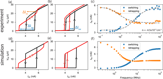
a I/V traces of the junction at bias frequencies of 0.1 MHz (red) and 100 MHz (black) in the regime where the effective AC amplitude is higher than the hysteresis. \(\Delta {I}_{{{\rm{re}}}}\) and ΔIsw highlight the change in retrapping and switching currents, respectively, between the two bias frequencies. b I/V traces of the junction at bias frequencies of 8 MHz (red) and 100 MHz (black) in the regime where the effective AC amplitude is higher than the hysteresis. The mismatch in retrapping current between the red and black curves is probably due to a charge jump (note it is of the order of a few pA). c Switching and retrapping currents as a function of AC bias frequency. d–f Numerical simulations of our device in the same regime as the data shown in (a–c). The grey dashed line in (c) is a fit to the functional forms provided in equations (1)–(3).
To extract the retrapping and switching rates, Γre and Γsw, for a given density from the experimental data, we fit the evolution of the retrapping and switching currents as a function of bias frequency. An analysis of the data, discussed in the Supplementary Information, demonstrates that both currents asymptotically approach a constant high-frequency value as 1/ω. To fit the results at all frequencies, we use the following functions: \({I}_{{{\rm{sw}}}}(\omega )={I}_{{{\rm{sw}}},\infty }-{I}_{RF}{\Gamma}_{sw}/\sqrt{{\Gamma}_{sw}^{2}+{\omega }^{2}}\) and \({I}_{{{\rm{re}}}}(\omega )={I}_{{{\rm{re}}},\infty }+{I}_{RF}{\Gamma} _{re}/\sqrt{{\Gamma}_{re}^{2}+{\omega }^{2}}\). That allows to characterize the corresponding rates (see Fig. 3(c), gray lines). The model described in Eqs. (1),(2),(3), reproduces correctly the asymptotic behavior of the switching current, while for the retrapping current the result depends on the particular form of IJ(T) (see Supplementary Information). For a fixed density in the junction, we extract the switching and retrapping currents for all frequencies and fit the results. In the example shown in Fig. 3(c), for a density of − 4.5 × 1012cm−2, we extract Γre = 0.52 MHz and Γsw = 2.75 MHz. Therefore, the weak-link dynamics of our junction gives us access to the quasiparticle thermalization rate and kinetic inductance of MATBG (Fig. 2c, d).
Physical interpretation of the frequency dependence
We now provide a physical interpretation of the rates, Γsw and Γre that allows us to connect them to the properties of MATBG. We begin with the switching rate Γsw. From Eq. (3) we identify the switching rate as Γsw = Rbulk/Lkin ∝ ns (see additional discussion in Supplementary Information). Assuming that the resistance of normal regions Rbulk does not strongly depend on T or bias strength, Γsw−1 ∝ Lkin, which allows to probe the superfluid stiffness of MATBG.
Before discussing the thermalization rate of the weak link, we note that for ω ≫ Γsw the AC part of the current does not reach the junction at all: Isc ≈ IDC. Thus, for Γre > Γsw, the kinetic inductance would set the rate for both switching and retrapping. However, as shown in Fig. 4, we have Γre strictly smaller than Γsw for all densities (note the different y-axis in Fig. 4a, c), confirming that we can interpret the former as a thermalization rate.
Fig. 4: Switching and retrapping rates and relative hysteresis across the phase diagram of MATBG.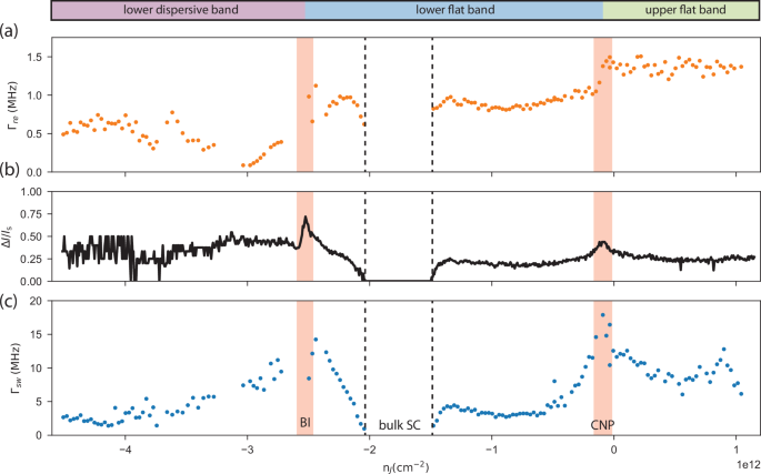
a Retrapping rate as a function of junction density. The region between vertical dashed lines represents the range of densities in which we have a bulk superconductor (SC). b Relative hysteresis as a function of junction density. We observe a peak at the charge neutrality point and another one at the band insulator between lower dispersive and flat bands. c Switching rate as a function of junction density. The red shaded areas highlight the regions in density where a transition between bands takes place. They correspond to the Charge Neutrality Point (CNP) and Band Insulator (BI).
Retrapping rate and thermalization
The equation governing thermalization in the device in Eq. (2) contains two implicit frequency scales: \(\gamma \equiv \frac{{G}_{{{\rm{th}}}}}{{C}_{{{\rm{el}}}}}\) and \(k\equiv \frac{{I}_{{{\rm{J}}}}^{2}{R}_{J}}{{C}_{{{\rm{el}}}}{T}_{{{\rm{J}}}}}\). Importantly, the hysteresis size for DC driving depends on their ratio γ/k (which is proportional to Gth, but independent of Cel), while the retrapping rate Γre depends on both, allowing in principle, to determine both scales.
These observations allow for a qualitative discussion of the results (Fig. 4(a,b)) across the MATBG phase diagram. The noticeable peaks in ΔI/Is, Fig. 4(b), occur near the band insulator (BI) and charge neutrality points (CNP) and indicate a suppressed thermal conductance Gth. This can be attributed to a lower density of states near these points compared to other concentrations, expected from previous experiments32,33 and theoretical analysis34. In contrast, Γre (Fig. 4(a)), which also depends on Cel (Fig. 4(a)) shows weaker features at these concentrations, indicating a simultaneous reduction of Gth and Cel, again consistent with a suppressed density of states. Remarkably, the minimum of Γre occurs for densities within the dispersive band. A potential explanation for this behavior is an increased resistance RJ due to the mismatch between flat-band electrons outside the junction and dispersive ones within it. Deeper into the dispersive band, this effect can be offset by an increased Gth.
The quantitative nature of Γre depends on the particular form of IJ(T); for the square-root model introduced above and γ/k \(\Gamma_{\mathrm{re}}=\frac{k\sin \frac{2\pi \gamma }{k}}{2\pi }\). Furthermore, the ratio between DC retrapping current and switching is \({I}_{{{\rm{re}}}}/{I}_{{{\rm{sw}}}}=\sqrt{\frac{\gamma }{k}}\) (see Supplementary Information). We stress that the observed Ir and Is are rather close to one another, which results in γ and k being effectively of the same order of magnitude. For larger values of γ the model predicts an 1/ω2 dependence of the retrapping current under AC bias; therefore the model should not be applicable for \({I}_{{{\rm{re}}}}/{I}_{{{\rm{sw}}}} \, > \, 1/\sqrt{2}\). However, in the absence of direct measurements of IJ(T), we will use this model to estimate Cel and Gth.
We observe, across the whole density range, three sets of values of Γre: 0.5 MHz, 1 MHz and 1.5 MHz, corresponding to the chemical potential of the link tuned to the dispersive band, lower flat band and upper flat band, respectively. The change in the hysteresis width, Fig. 4(b) is relatively smaller. Using the analytical formula given above, we can estimate for ΔI/Isw ≈ 0.5 that γ ≈ 0.8−2.3 MHz. Reference22, where laser-mediated heating of a MATBG sample allows for the extraction of the same quantity, reports a value of γ ≈ 2 MHz. The fact that such different methods for extracting the thermalization rate agree on the obtained value strengthens both of them as reliable characterization tools.
This result already provides an important insight into the low-temperature behavior of electron-phonon coupling in MATBG when contrasted with those at higher temperatures. In particular, the cooling rate has been found to be of the order of hundreds of GHz above 5 K with a very weak temperature dependence23, attributed to effective moiré umklapp scattering35 (that is related to folding of the acoustic phonons by the moiré lattice) explaining the linear-in-temperature resistivity4,10,35. The strong difference with our result at T ~ TJ ≈ 100 mK suggests a suppression of the cooling rate much stronger than linear-in-temperature. This result is consistent with electron-phonon scattering at 100 mK being in the Bloch-Gruneisen regime where umklapp scattering is suppressed35 and resistivity from electron-phonon scattering should follow a stronger power-law dependence on temperature36. This excludes electron-phonon scattering as the origin of linear-in-temperature resistance at low temperatures37.
In the case of superconductivity, the most relevant quantity when discussing electron-phonon coupling is the dimensionless coupling constant, which we note here λ. The temperature relaxation rate at low temperatures is related to the strength of the coupling to acoustic phonons38,39,40. While this coupling does not take the contribution of optical phonons into account, it is expected to be of the same order of magnitude as the full coupling constant38. To obtain an estimate we use a Dirac electron model4,39,40, motivated by the theoretical34 and experimental evidence32,33 for their presence in MATBG bands, in particular in the vicinity of CNP (consistent with the peak in ΔI/Is discussed above). One finds that \(\gamma=\frac{{G}_{{{\rm{th}}}}}{{C}_{{{\rm{el}}}}}=\lambda \frac{16{\pi }^{2}}{5}\frac{{({k}_{B}{T}_{el})}^{2}}{{\hslash }^{2}s{k}_{F}}\), where s is the acoustic phonon velocity. Using Tel ~ TJ ~ 0.1 K from the extinction temperature of SQUID oscillations19, s ≈ 20 km/sec (the value for single-layer graphene41 is expected to be close to that in MATBG42), \({k}_{F}=\sqrt{\pi n}\) for n ~ 1 × 10⁻¹² cm−2 and γ ~ 1 MHz we obtain λ ~ 10−3. Several comments are in order regarding this estimate of λ. We begin by stressing this estimate may not be directly comparable to other transport measurements (e.g., resistivity) as our estimates of λ stem from the electron-phonon cooling rate. While the relation between the way electron-phonon coupling enters the cooling rate, the resistivity, and the superconducting pairing is established in the Dirac model4,39,40, it is yet to be determined (and may be different) in the MATBG bands. Moreover, the potential inhomogeneity of the twist angle across the sample may reduce the average thermal relaxation rate, since regions that are away from the magic angle are expected to have lower density of states and thus slower thermal relaxation. Additionally, the above estimate is assuming the system is in the Bloch-Gruneisen regime T ≪ cskF; it has been however demonstrated35,43 that the crossover to this regime may be quite different in MATBG than in single-layer graphene and, in particular, it occurs at much lower temperatures. In fact, the strong reduction of the thermal relaxation rate in our experiments with respect to the values at 5 K23 may present a first demonstration of this crossover occurring in MATBG. We note that this estimate assumes coupling to lowest-energy acoustic phonons only, and does not address optical or any other phonons that are frozen out at the experimental temperatures. Finally, the Dirac model should be applicable only around certain fillings; in our case, a signature of Dirac physics is observed near the CNP in enhanced ΔI/Is indicating less efficient heat relaxation due to lower density of states near a Dirac point.
We can further estimate Gth and Cel taking IJ − Iexc ~ 5 nA, ΔV ~ 20 μV from Fig. 3. The result is Gth ~ 250 fW/K and Cel ~ 5 × 10¹⁹ J/K. From the junction area and n ~ 1 × 1012 cm−2 one expects above 103 electrons, with the usual Sommerfeld expression \({C}_{{{\rm{el}}}}=\frac{{\pi }^{2}}{2}kN\frac{{k}_{B}T}{{E}_{F}} \sim 1{0}^{-19}\frac{{k}_{B}T}{{E}_{F}}\) J/K. In usual metals, \(\frac{{k}_{B}T}{{E}_{F}}\ll 1\), while in our case this implies \(\frac{{k}_{B}T}{{E}_{F}} \sim 1\), that may be related to large residual entropy of interacting states of MATBG44,45. Both Gth and Cel are much higher than those expected in monolayer graphene40, consistent with strongly suppressed bandwidth and electron velocities of MATBG \(G\propto {v}_{F}^{-2},C\propto {v}_{F}\). However, the \(\gamma=\frac{{G}_{{{\rm{th}}}}}{{C}_{{{\rm{el}}}}}\) we find in MATBG at T ≈ TJ are of the same order as those predicted for monolayer graphene40.
Switching rate and superfluid stiffness
We now discuss the switching rate Γsw (Fig. 4c), related to the superfluid stiffness in the bulk of our MATBG device. Importantly, the AC measurements are still performed at a finite DC bias, thus, our measurements reveal the superfluid density at a finite current bias, ns(IDC) ≈ ns(Isw). Since ns(Isw) is a decreasing function of current, the steep increase in Γsw at the edges of the lower flat band is explained by the decreasing critical current of the junction (Fig. 1 (d)). On the contrary, the decrease of Γsw for densities in the top flat and dispersive bands, is unexpected – at such low critical currents ns(Isw) ≈ ns(0) should be density-independent and large. We suggest that this observation can be explained by the kinetic inductance of proximity-induced superconductivity in the junction region. Being very weak, the proximity-induced superfluid has an extremely large kinetic inductance that is in parallel to the smaller one from the bulk TBG, effectively shunting it. Furthermore, since Γsw ∝ Rbulk, changes in the resistance with concentration can also affect its magnitude. In particular, this provides a plausible explanation of the peak of Γsw near CNP, where the normal-state resistance peaks.
Let us now return to the densities within the lower flat band, where Γsw is related to the superfluid density of bulk MATBG. The dependence of Γsw ∝ ns as a function of IDC, shown in Fig. 5, gives important information about the nature of the superconducting gap in MATBG. Current biasing a superconductor produces a Doppler shift46,47 of the quasiparticle bands in a superconductor, see inset of Fig. 5 (ΔE = vs × ℏk, where vs is the superfluid velocity and k the quasiparticle momentum). For an isotropic superconductor, depicted in the inset of Fig. 5, this does not affect the quasiparticle occupations until a critical value of bias current is reached. As a result, ns(I) dependence is highly nonlinear with an abrupt drop close to the critical current48. For a highly anisotropic or nodal superconductor, across its nodal axis in real space, the quasiparticle band structure presents cones instead of a gap in density (Fig. 5, inset). A small shift originating from a finite bias current, leads to a finite generation of quasiparticle pairs, thus reducing the superfluid density before breaking down the superconducting condensate. As Fig. 5 shows, the relation between superfluid density and bias current is linear in the case of MATBG in the range Idc ∈ [0.6Ic, 0.95Ic]. This result is inconsistent with the behavior expected of an isotropic superconducting gap, ruling in favor of a highly anisotropic or nodal pairing state in MATBG.
Fig. 5: Superconducting stiffness in arbitrary units as a function of bias current to critical current ratio.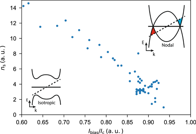
Inset, bottom left: Schematics of Bogoliubov-de Gennes quasiparticle band structure of a superconductor with isotropic gap. The solid straight line represents the Fermi energy at zero current bias. The dashed line represents the Fermi energy at a non-zero current bias. Inset, top right: Schematics of quasiparticle band structure of a superconductor with anisotropic gap. The red and blue areas represent respectively the hole and electron pockets that form at the band edges under a finite current bias.