Device configuration of CLCN-integrated vdW CPL detectors
Figure 1a illustrates the configuration and operational principles of our device. We have developed a CPL detector that incorporates a CLCN film atop a 2D MoTe2/MoS2 photodiode. The detector identifies CPL via a two-step process: first, it reflects CPL within a specific wavelength range through the CLCN film, and second, it absorbs transmitted light and separates photogenerated carriers with the semi-vertical MoTe2/MoS2 heterostructure. The MoTe2 and MoS2 serve as p-type and n-type semiconductors, forming a staggered (type II) p-n diode structure. The fabricated CLCN film is dry transferred onto the vdW p-n diode, as confirmed by optical microscopy in Supplementary Fig. 1. To evaluate the CPL-selective properties of our device, we first investigated the transmission of CPL through R-form and S-form configurations of the CLCN film. In the 900–950 nm near-infrared (NIR) region, the R-form CLCN film transmits left-handed circularly polarized light (LH-CPL) while reflecting right-handed circularly polarized light (RH-CPL), whereas the S-form CLCN film exhibited the opposite behavior (Fig. 1b). The dissymmetry factors of the CLCN films were calculated as 1.89 for the R-form and −1.88 for the S-form. The strong chiral optical response was further validated by circular dichroism spectra, which exhibited an ellipticity of approximately 20° at the target wavelength (920 nm) (Supplementary Fig. 2)20. Thickness effects of CLCN films were also examined. As the thickness of the R-form CLCN increases, the transmittance for both RH-CPL and LH-CPL decreases. Consequently, the variations in g-factor values remain insignificant (Supplementary Fig. 3). Additionally, the CPL wavelength selectivity can be tuned from the visible to the NIR range by adjusting the helical pitch, which depends on the concentration of the chiral dopant (Supplementary Fig. 4)19. Next, we investigated light absorption and carrier separation in a semi-vertical structured vdW p-n photodiode that integrates a Pt bottom electrode directly under the MoTe2/MoS2 heterostructure (Fig. 1c). This arrangement enhances light absorption and facilitates the collection of photogenerated carriers by minimizing the quasi-neutral area that generates parasitic resistance, thus improving photoresponse speed21,22. The band structure of the semi-vertical p-n diode under equilibrium conditions is depicted in Fig. 1d, where the values of the bandgap and sub-bandgap due to intercoupling effects at the heterostructures were confirmed in our previous work22. Given that the Fermi level of MoS2 is at a higher energy compared to MoTe2 (∆EF = ~ 0.08 eV), electrons from MoTe2 naturally migrate towards MoS2, creating a built-in potential at their junction22. Upon illumination of the heterostructure, photogenerated carriers are efficiently separated by the built-in electric field within the junction area. Strategic placement of the Pt electrode near the vdW heterojunction facilitates the direct collection of these separated carriers, thus enabling a rapid photoresponse. Characterization of our devices was performed using optical microscopy to assess the geometrical configuration, atomic force microscopy to measure thicknesses, and Raman spectrometry to analyze crystallinity (Fig. 1e and Supplementary Fig. 5)23. As a control benchmark for integrating the CLCN film, the spectral responsivity of a MoTe2/MoS2 p-n diode without CLCN film was evaluated in Fig. 1f. The device exhibited a broad detection capability, ranging from the visible to the NIR spectrum (400–1300 nm). This range is nearly compatible with the possible reflection wavelength range of the CLCN film (300–1100 nm)19. Upon integrating R-form and S-form CLCN films, a decrease was observed in the responsivity of the R-form CIP towards RH-CPL and of the S-form CIP towards LH-CPL (Fig. 1g). Remarkably, the responsivity profiles of the devices integrated with either R-form or S-form CLCN film for CPL were found to be similar to the responsivity spectrum of the control benchmark sample. This indicates that the integrated CLCN film selectively attenuates the responsivity to specific circular polarizations without significantly affecting the overall detection capabilities of the device across its operational spectrum. We also examined spectral photoresponse measurements of R-form CIPs integrated with CLCN films designed for reflection of 520 nm and 830 nm light, explicitly demonstrating that responsivity in other wavelength ranges can also be selectively attenuated. (Supplementary Fig. 6). Our device concept was validated by mapping spatial photocurrents in the CIPs, as shown in Fig. 1h (R-form) and Fig. 1i (S-form). The variation in spatial photocurrents influenced by CPL chirality demonstrates the effectiveness of the CLCN film, indicating that the p-n junction, particularly in the semi-vertical region where the bottom electrode overlaps, is the predominant site for photocarrier generation.
Fig. 1: Characterization and performance evaluation of a CPL detector incorporating CLCN film.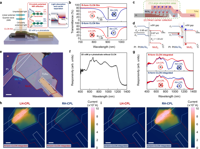
a Schematic representation of a circularly polarized light (CPL) detector detailing the operational principle of the device, where selective reflection and absorption of CPL are achieved via cholesteric liquid crystal network (CLCN) film and MoTe2/MoS2 heterostructure, respectively. b Transmission efficiency of CPL through R-form and S-form configurations of the fabricated CLCN film. c Schematic representation of a semi-vertical MoTe2/MoS2 structure, highlighting an effective operational strategy. d Band structure of a semi-vertical van der Waals (vdW) MoTe2/MoS2 p-n diode. e Optical microscopy image of a MoTe2/MoS2 semi-vertical van der Waals p-n diode. Scale bar is 10 µm. f Spectral responsivity of a MoTe2/MoS2 p-n diode without CLCN film, serving as a control benchmark. g Responsivity profiles of R-form and S-form CLCN-integrated photodiodes (CIPs). Photocurrent mapping in (h), R-form and (i), S-form CIPs, respectively. Each panel shows the response under left-handed circularly polarized light (LH-CPL) on the left and right-handed circularly polarized light (RH-CPL) on the right. Scale bar is 10 µm.
Photodiode characteristics of CLCN-integrated photodiodes
Next, considering the spectral photoresponses of the R-form and S-form CIPs, a 904 nm NIR laser diode was chosen as the light source, and the CPL detection characteristics of both forms of CIPs were examined. For the R-form CIP, a significant photovoltaic effect was observed for LH-CPL, where the open-circuit voltage (VOC) was 0.24 V and the short-circuit current (ISC) was −88.5 nA (Fig. 2a). In contrast, a relatively low photovoltaic effect was observed for RH-CPL in this device, with a VOC and ISC of 0.07 V and −3.4 nA, respectively (Fig. 2b). Conversely, the S-form CIP revealed opposite selectivity, exhibiting weaker photovoltaic effect for LH-CPL with a VOC and ISC of 0.08 V and −4.2 nA, while showing a much more pronounced photovoltaic effect for RH-CPL with a VOC of 0.22 V and ISC of −72.2 nA, respectively (Fig. 2c, d). The difference in photovoltaic properties for CPL is due to the chiral-selective reflection of the R-form and S-form CLCN films. Statistical analysis of several batches of CIPs revealed that ISC exhibited a near-linear relationship with active volume of CIPs (Supplementary Fig. 7). Our device exhibited a nearly ideal (linear) photoresponse to incident optical power density for both R-form and S-form CIPs in photovoltaic mode (V = 0 V, without external bias). The linearity parameter (α) was extracted from photocurrent variations as a function of optical power density, as shown in Fig. 2e, f, determined to be approximately 1 for both LH-CPL and RH-CPL. This outcome indicates the absence of complex carrier generation, trapping, and recombination processes within typical semiconductors21. The overall equations for extracting the device parameters are given in the Methods section. The linear photoresponse was observed across a wide optical power range. The R-form CIP demonstrated a linear dynamic range of 110.3 dB / 71.3 dB for LH-CPL / RH-CPL, while the S-form CIP correspondingly reached 91.4 dB/114.1 dB. In this range, the responsivity maintained a nearly constant value, as depicted in the insets of Fig. 2e, f, which is particularly advantageous for applications requiring precise detection such as imaging. Almost independent of optical power density in the detectable range, the g-factor values were calculated as 1.88 for the R-form and −1.90 for the S-form CIPs (Supplementary Fig. 8). Notably, the dissymmetry factors of the CIPs are in close agreement with those observed in the CLCN (1.89 for the R-form and −1.88 for the S-form), attributable to the linear photocurrent response of the vdW photodiode to optical power density. The specific detectivity (D*) of R-form and S-form CIPs was estimated to be approximately 108 Jones (cmHz0.5W−1), as estimated from the noise power spectral density (refer to Supplementary Fig. 9). External quantum efficiency (EQE) values were also examined, showing 26.7% for LH-CPL in the R-form CIP and 26.31% for RH-CPL in the S-form CIP.
Fig. 2: Comprehensive analysis of CPL detection capabilities of CLCN-integrated photodiodes.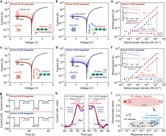
I-V characteristics when (a), LH-CPL and (b), RH-CPL are applied to an R-form CIP. I-V curve when c, RH-CPL and (d), LH-CPL are applied to an S-form CIP. Extracted photoresponse with respect to optical power density in photovoltaic mode for the (e), R-form CIP and (f), S-form CIP. g Time-resolved photoresponse of R-form and S-form CIPs to alternating RH-CPL and LH-CPL. h Rise and fall times of CIPs for CPL. i Benchmarking results of dissymmetry factor and photoresponse time with other CPL detectors.
Compared with phototransistors, which show high responsivity as photodetectors owing to their photoconductive gain, photodiodes exhibit significantly faster operation speed. To investigate the dynamic characteristics of our devices, CIPs were exposed to alternating pulses of RH-CPL and LH-CPL (Fig. 2g). In the R-form CIP, photocurrent with LH-CPL was significantly higher than with RH-CPL, while conversely, the S-form CIP displayed much higher photocurrent under RH-CPL compared to LH-CPL, with neither case exhibiting a notable memory effect. The device showed stable operation up to 500 cycles, with a cycle-to-cycle variation of 0.046% (Supplementary Fig. 10). Next, both R-form and S-form CIPs exhibited rapid photocurrent-switching characteristics. Frequency modulation up to 10 kHz resulted in rise and fall times of 4 μs and 4 μs, respectively, for LH-CPL with the R-form CIP and RH-CPL with the S-form CIP. Based on the finding that vdW p-n photodiodes with and without CLCN film exhibited similar photoresponse times, we concluded that CLCN film integration does not compromise the high performance of vdW p-n photodiodes in terms of photoresponse time (Fig. 2h). The devices also exhibited cut-off frequencies exceeding 100 kHz in photovoltaic mode (Supplementary Fig. 11). The performance comparisons between our CIPs and other CPL detectors in Fig. 2i and Supplementary Table 2 highlight the high dissymmetry factor and rapid photoresponse time of the CIPs. Such results demonstrate the benefits of integrating the highly selective polarization detection capability of CLCN film with the efficient light absorption and carrier separation capabilities of vdW p-n photodiodes7,9,14,15,17,20,24,25,26,27,28,29,30,31,32,33,34,35.
Chiral decomposition and image recognition of mixed circularly polarized images
To evaluate the discrimination capability of the CPL detector, we assess the device’s capability to decompose mixed circularly polarized (CP) images containing both LH-CPL and RH-CPL. Decomposition of mixed optical signals components is commonly applied to obtain clear image signals in various fields5,6,7,8,9,10. However, this cannot be achieved through a software-based approach in cases employing achiral photodetectors. When light composed of equal parts LH- and RH-CPL is irradiated onto photodiodes, achiral photodetectors capture both polarizations, leading to images that lose chiral information. In contrast, an R-form CIP filter captures only LH-CPL, while an S-form CIP captures only RH-CPL, allowing a distinct image of each CP component to be obtained, as shown in Fig. 3a (right). In an evaluation of CP imaging for image recognition, the capturing of both chiral signals by achiral photodiodes may lead to misrecognition, for example mistaking the combined signal of “2” and “5” numerals for an “8” as shown in Fig. 3b. In contrast, R-form and S-form CIPs effectively distinguish the specific chiral signals from mixed CPL, enabling accurate recognition of “2” and “5”, respectively.
Fig. 3: Chiral decomposition and image recognition of mixed circularly polarized images.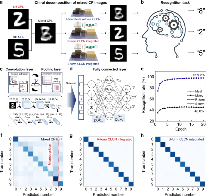
a Selective detection of LH-CPL and RH-CPL by R-form and S-form CIPs, enabling distinct image components to be captured. b Comparison of image recognition. Conventional photodiodes blur mixed circularly polarized (CP) signals, leading to errors, whereas CIPs accurately distinguish and identify overlapped numerals, enhancing recognition accuracy. c Detailed segment of the convolutional neural network (CNN) architecture used for feature extraction, emphasizing convolution, pooling, and rectified linear unit (ReLU) activation functions. d Classification process facilitated by the fully connected layer. e Comparison of image recognition rates underscoring the superior performance of CIPs for mixed CP images. f Confusion matrix for mixed CP images, with subsequent matrices for images processed by (g), R-form and (h), S-form CIPs demonstrating improved recognition capabilities.
To further confirm this, we prepared a modified MNIST test dataset in which each image is added to the next image to simulate mixed CPL (Mixed CPL in Fig. 3a). Here, we assume that the former image indicates LH-CPL and the latter image indicates RH-CPL. We then emulated image acquisition by R-form and S-form CIPs using the fitted responsivity obtained from Fig. 2e, f, respectively. The images processed from mixed CPL by each device are compared in Supplementary Fig. 12. The recognition rates of these processed images were then evaluated using a CNN trained with the MNIST training dataset using Python with TensorFlow. The architecture of the software-based algorithm consisted of sequential layers aimed at progressively extracting and refining feature maps. We used a stack of convolutional layers with ReLU activations to introduce nonlinearity, followed by max-pooling and batch normalization to improve training stability and convergence speed (Fig. 3c top). In detail, a 3 × 3 convolutional kernel was applied with 64 filters to detect low-level features, such as edges and corners. This layer was followed by a second 3 × 3 convolution layer with 64 filters, also using the ReLU activation function. After each convolutional block, a 2 × 2 max-pooling layer down-sampled the feature maps, reducing the spatial dimensions while preserving key information. Subsequent layers increased the filter depth, with two additional convolutional layers, each containing 128 filters and a 3 × 3 kernel size, which captured more complex patterns and spatial hierarchies within the images. Another max-pooling and batch normalization layer followed, enhancing the robustness of feature extraction across different training batches. A final convolutional layer with 256 filters applied further refinement, allowing the model to capture high-level abstract features (Fig. 3c bottom). The output from the convolutional blocks was flattened into a one-dimensional vector and passed through a fully connected layer with 512 neurons and a ReLU activation function, enabling the model to learn intricate representations for classification. The final layer consisted of a 10-neuron softmax layer, outputting the probability distribution for each digit class from 0 to 9. We optimized synaptic weights using the Adam optimizer with a learning rate of 10−5, minimizing the categorical cross-entropy loss over 20 epochs (Fig. 3d). Over 20 training epochs, simulated images processed with both R-form and S-form CIPs achieved a maximum recognition rate of 98.2%, matching the ideal rate obtained with clean MNIST dataset (Fig. 3e). In contrast, the recognition rate for mixed CP images was significantly lower at 45.1%. The discrepancies between predicted numbers and true numbers for each image are depicted using confusion matrices, showing clear enhancement of image recognition capabilities. The confusion matrix for mixed CPL in Fig. 3f revealed significant mispredictions, particularly in misclassifying the value “8”. In contrast, as shown in Fig. 3g, h, images captured using photodiodes integrated with both R-form and S-form CIPs demonstrated a marked improvement in accurate recognition. To test the broader applicability of the CIPs, we conducted the same process with a more complex dataset, Fashion-MNIST. Similarly as above, image processing using R-form and S-form CIPs resulted in clearly separated images (Supplementary Fig. 13). In subsequent recognition tests, the processed images achieved recognition rates of 88.0% and 87.8% for the R-form and S-form CIPs, respectively, closely approximating the rate of 88.5% obtained with the clean dataset (Supplementary Fig. 14).
Zero- and one-dimensional mixed-multimodal image processing
Conventional in‐sensor computing relies on an all‐reconfigurable‐device configuration that maps responsivity values to kernels via the electrostatic doping effect using additional gate terminals11,36. Replacing these reconfigurable devices with non-reconfigurable ones with fixed responsivity enables the same (but non-reconfigurable), kernel operation while significantly reducing the extra circuit elements required for responsivity tuning; however, non-reconfigurable kernel operation lacks the optimization capability necessary for more effective image processing. In this context, in‐sensor dynamic computing replaces only a subset of the reconfigurable devices with non-reconfigurable ones. Although this approach reduces universality, it still maintains image processing optimization through reconfigurable responsivity tuning, consequently reducing circuit complexity4. Inspired by these advancements, we propose a universal approach that enables the dynamic blending of two kernel operations within an all‐non-reconfigurable device configuration by continuously adjusting the polarization states of light. Our method retains kernel optimization capabilities while significantly reducing circuit complexity compared to current in-sensor technologies (Supplementary Fig. 15).
To implement polarization-sensitive, in-sensor mixed-multimodal processing with the aid of our CIPs that exhibit a combination of good linearity, high dissymmetry factor, and fast dynamic speed, we examined the photoresponse of CIPs to the continuous modulation of LH-CPL and RH-CPL, a crucial aspect of in-sensor mixed-multimodal image processing. The top panel of Fig. 4a illustrates the generation of various light polarizations, ranging from circular to linear, by adjusting the angle of a half-wave retarder (θ). Here, incident light undergoes polarization through a linear polarizer, after which the polarization direction is modified by rotating a half-wave retarder, causing a 2θ rotation of the polarization direction for every θ rotation of the retarder. The rotated linearly polarized light, when passing through a subsequent quarter-wave retarder, adopts either linear or circular polarization, contingent upon its angle concerning the optical axis of the quarter-wave retarder. Additional details on this polarization adjustment process involving half-wave and quarter-wave retarders are provided in Supplementary Fig. 16. The bottom panel of Fig. 4a displays the transition of polarized light, representing the change from linear to circular polarization. We next examined the photoresponsivity of both R-form and S-form CIPs depending on the rotated angle of linear polarized light. As depicted in Fig. 4b, despite the non-reconfigurable functionality of the CIPs, the polarized light, varying from linear to circular polarization, induced dynamic changes in photoresponsivity. In the case of CPL, R-form and S-form CIPs exhibited opposite polarimetric responsivities: maximum for left-handed polarization in the R-form CIP and minimum in the S-form CIP, with the roles reversed for right-handed polarization. For linearly polarized light, the polarization angle was irrelevant to the responsivity due to the inherent rotational symmetry of CLCNs. Moreover, responsivity values for elliptically polarized light, interpolating between linear and circular polarization, showed a distinct sinusoidal dependence on the linear polarization angle (2θ). The time-dependent photocurrent for both R-form and S-form CIPs demonstrated consistent behavior under uniform rotating speed of half-wave retarder (Fig. 4c). This continuous and opposing modulation of responsivity in the chiral opposite CIPs facilitates mixed-multimodal image processing.
Fig. 4: Zero- and one-dimensional mixed-multimodal image processing.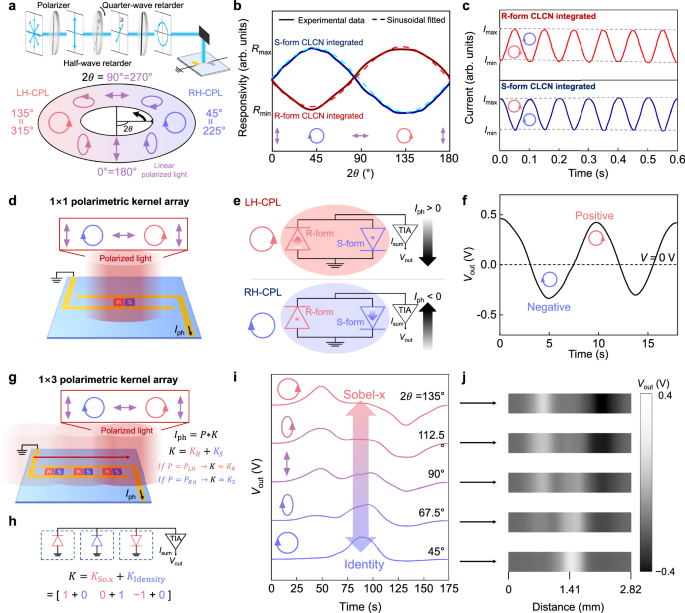
a (Top) Illustration of polarized light generation methods transitioning from circular to linear polarization. (Bottom) Display of polarized light variations achieved through the adjustment of the angle of a half-wave retarder. b Responsivity of R-form and S-form CIPs to linear and circularly polarized light. c Time-resolved photocurrent measurements to characterize R-form and S-form CIP behavior with a half-wave retarder rotating six times at a uniform speed. d Schematic of a 1 × 1 polarimetric array with integrated localized CLCN on vdW photodiodes. e Photocurrent behavior of the 1×1 array under LH-CPL and RH-CPL illumination. f Vout of the 1 × 1 array as the polarization state varies. g Schematic of a 1 × 3 polarimetric array illustrating analog convolution of incident light and CIP responsivities. h Circuit illustration polarimetric kernel consisting of Sobel-X (R-form) and identity (S-form). i Measured voltage signal over time during a 904 nm spot scan across the array under different polarizations. j Spatially processed voltage signals by polarimetric kernel array.
As proof of concept, we fabricated a simple zero-dimensional (1 × 1) polarimetric array of CIPs with a kernel value of +1 (identity) for the R-form CIP and –1 (negation) for the S-form CIP (Fig. 4d). In this configuration, two devices connected in parallel simultaneously generate photocurrents in opposite directions in photovoltaic mode (V = 0 V), which are summed according to Kirchhoff’s law. This accumulated current is then converted to voltage using a transimpedance amplifier (TIA) for practical use11. An optical microscopic image of zero-dimensional polarimetric array is presented in Supplementary Fig. 17. Each device selectively absorbs light of different polarization, resulting in a positive photocurrent under LH-CPL illumination and a negative photocurrent under RH-CPL illumination (Fig. 4e). Figure 4f shows the output voltage (Vout) of the 1 × 1 polarimetric array, where the polarization state varies by rotating the half-wave retarder. As the polarization state changes, Vout dynamically varies from negative to positive without the need for an additional responsivity control terminal.
Next, we fabricated a one-dimensional (1 × 3) polarimetric array of CIPs to demonstrate the polarization-sensitive, in-sensor mixed multimodal imaging process for a cross section of light. In this configuration, as a light spot traverses the entire 1 × 3 photodiode array from left to right, analog convolution between the 1 × 3 incident polarized light power (P) and the programmed 1 × 3 responsivity (K) for each CIP produces individual currents that sum according to Kirchhoff’s current law. (Fig. 4g). Here, the parameter K can dynamically vary from KR to KS, depending on the applied polarized state of light and the degree of superposition between LH-CPL and RH-CPL. The polarimetric kernel is designed as a Sobel-X filter using R-form CIPs and as an identity filter using S-form CIPs, while the TIA converts the accumulated currents into Vout (Fig. 4h). For the application, we implemented localized CLCN directly integrated on vdW photodiodes (Supplementary Fig. 18). The fabrication process of localized CIPs is shown in Supplementary Fig. 19. The transmittance of the CLCN fabricated using this method, along with the photoresponse of the directly integrated CIPs, confirmed sufficient circular polarization detection capability up to microscale size (Supplementary Figs. 20 and 21). Figure 4i illustrates the measured Vout over time as 904 nm light is scanned from left to right across the polarimetric kernel array. Under LH-CPL illumination, both positive and negative voltage responses are observed when the edge of the light spot crosses the kernel. In contrast, under RH-CPL illumination, only positive voltage response is observed as the center of the light spot traverses the kernel. By adjusting the half-wave retarder angle (2θ), a mixed polarization state is generated, resulting in a superposition of the two voltage responses. Given the measured light velocity of 16.21 µm s−1, these results can be interpreted in terms of one-dimensional spatial imaging for cross-section of incident light (Fig. 4j). The processing function transitions from an identity operation to Sobel-X filtering based on the polarization state, successfully demonstrating polarization-sensitive, in-sensor mixed multimodal computing.
Two-dimensional polarization-sensitive mixed-multimodal imaging
Based on the above result, we conceptually constructed a 3 × 3 polarimetric kernel array for a polarization-dependent, mixed-multimodal image processor to demonstrate the potential of our device for mixed-multimodal imaging. (Fig. 5a). The kernel array consists of CPL photodiodes connected in parallel for convolution operation, where the responsivity values corresponding to the kernel matrix are determined by their number and positions. By adjusting the polarization state, the programmed kernel values can be continuously tuned, spanning kernels matrix configured from R‐form CIPs to those with S‐form CIPs. Here, the analog convolution between the 3 × 3 incident polarized light power (P) and the programmed 3 × 3 responsivity (K) for each CIP produces individual currents that sum according to Kirchhoff’s current law. The parameter K can dynamically vary from KR to KS, depending on the applied polarized state of light and the degree of superposition between LH-CPL and RH-CPL. A system for generating continuous polarized images and subsequent processing by a mixed-multimodal image processor, consisting of a 3 × 3 polarimetric kernel array, is shown in Fig. 5b, where the generation of a polarized image follows the explanation in Fig. 4a. The image utilized here illustrates common intensity information, and our system performs mixed-multimodal processing by polarizing this intensity information and subsequently processing it using polarization-sensitive kernels.
Fig. 5: Two-dimensional polarization-sensitive mixed-multimodal imaging.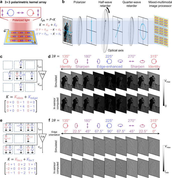
a Layout of a 3 × 3 polarimetric kernel array designed for polarization-sensitive image processing, enabling distinct detection and processing of images based on polarization chirality. b System depiction of continuous polarized image generation and subsequent processing via a 3 × 3 polarimetric kernel array, illustrating the concept of polarization-sensitive in-sensor mixed-multimodal imaging. c Circuit illustration for polarimetric kernels consisting of identity and edge-enhancement operation. d Comparison of simulated results (assuming an ideal dissymmetry factor of 2) and in-sensor computed emulation, showing the seamless transition from identity filtering to edge-enhanced imaging with varying polarization angles using the Cameraman image. e Circuit illustration for polarimetric kernels consisting of identity and edge-enhancement. f Transition of processed image from Sobel-X to Sobel-Y processed images with changing polarization angles, enabling angle-dependent edge detection. The Cameraman image is adapted from (© Massachusetts Institute of Technology, used under the CC BY-NC 4.0 license).
To test the versatility of this concept we investigated three distinct mixed-multimodal imaging techniques: identity with edge-enhanced features, Sobel-X and Sobel-Y, and a combination of blurring and sharpening. In each case, we combined kernel arrays with R-form and S-form photodetectors to generate mixed kernels. The circuit diagram in Fig. 5c depicts the generation of an output signal from a mixed kernel, integrating identity and edge enhancement, through the summation of currents from two distinct 3 × 3 polarization-sensitive photodetector arrays4. We note that Vout is set to zero if Vout is less than zero4. We compared the simulated result (which assumes an ideal dissymmetry factor of 2) with an in-sensor computed one using a widely utilized stock photo known as the Cameraman image. Here, the mixed-multimodal image processor used the fitted responsivity obtained from Fig. 2e, f. Applying polarization states that vary with the polarization angle (2θ), seamless transitions of the processed image from identity filtering to edge-enhanced imaging were achieved, as shown in Fig. 5d and Supplementary Video 1. Identity filtering preserves the static features of an image, while edge enhancement accentuates boundaries and transitions to highlight dynamic features. By continuously blending these two techniques—from identity to edge detection—through polarization modulation, we anticipate high applicability in fields requiring the analysis of both static and dynamic elements, like autonomous driving4. Compared to the simulated result, the in-sensor computed result exhibits partial mixing between the two kernels even under conditions of unmixed polarization, which is due to the incomplete suppression of photocurrent generation from untargeted CPL devices. Nonetheless, the high dissymmetry factor of the CPL device does not critically compromise the result. Figure 5e presents another mixed-multimodal image processing method that uses a circuit diagram to process Sobel-X and Sobel-Y kernel combinations. The distinction between this method and that in Fig. 5c lies in the configuration of the photodetectors along different kernel matrices. As the angle of the polarized light to the quarter-wave plate shifts from 135° to 225°, the processed image exhibits a seamless transition from Sobel-X to Sobel-Y processing, enabling angle-dependent edge detection from 0° to 90° (Fig. 5f). The third application, i.e., blurring and sharpening, is explored in Supplementary Fig. 22. Specifically, the blurring kernel effectively reduces noise but diminishes image contrast, whereas the sharpening kernel enhances contrast yet can amplify noise. By optimally mixing these two kernels, the method achieves a targeted compromise between noise reduction and contrast enhancement. Following confirmation of the universality of mixed-multimodal image processing, the potential to dynamically optimize the mixed-kernel techniques can be explored. Although our work validated potential of polarimetric 3 × 3 kernel operation through emulation, a realistic implementation of a large-scale 3 × 3 array-level mixed multimodal computing system can be achieved through two key advancements: (i) the development of p-n diodes based on uniformly grown large-area vdW films and (ii) equipment capable of precisely depositing CLCN liquid in defined quantities and positions37. Template-assisted processing of the CLCN liquid, combined with capillary-driven injection can be employed for the micro-patterning of CLCN38. We are currently in the preparatory stage of implementing a 3 × 3 array using large-area vdW films (Supplementary Fig. 23). By integrating precise localized-CLCN printing technology with fabricated large-area vdW p-n films, we anticipate that a large-area polarimetric kernel array composed of low-variation CIP elements can be realized.