Scientists at the University of Warwick and the National Research Council of Canada say they have achieved the highest electrical conductivity ever recorded in a silicon-compatible material, marking what they describe as a major step toward faster, more efficient electronic and quantum devices.
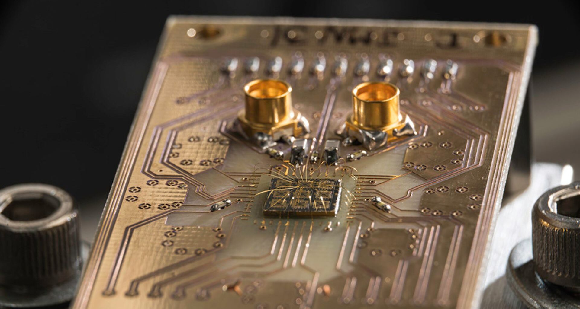
The breakthrough, published this week in Materials Today, centers on a nanometer-thin, compressively strained germanium layer grown on a silicon wafer.
The material allows electrical charge to move through it with unprecedented ease, potentially extending the life of silicon-based chip manufacturing as the semiconductor industry confronts the physical limits of modern processors.
New quantum semiconductor material
Most chips today still rely on silicon, but as components shrink and transistor densities rise, modern devices generate more heat and face diminishing returns on performance.
Germanium, used in the earliest transistors of the 1950s, has long been known to offer superior charge mobility but has been difficult to integrate with mainstream silicon production techniques.
Dr. Maksym Myronov, an associate professor at Warwick and head of the university’s Semiconductors Research Group, said the team’s new germanium-on-silicon material, known as compressively strained germanium on silicon (cs-GoS), overcomes that barrier.
“Traditional high-mobility semiconductors such as gallium arsenide are very expensive and cannot be integrated with modern silicon manufacturing,” Myronov said in a statement.
“Our new CS-GoS quantum material combines world-leading mobility with industrial scalability, a key step toward practical quantum and classical large-scale integrated circuits.”
Researchers achieved the performance gains by applying controlled compressive strain to an ultrathin germanium layer.
That process creates an extremely pure, orderly crystal structure, reducing imperfections that slow the flow of electrical charge.
Measurements show the material reached a record hole mobility of 7.15 million square centimeters per volt-second, many times higher than standard industrial silicon and the highest value ever reported for a group-IV semiconductor compatible with modern chip fabrication.
Breaking the conductivity record
Dr. Sergei Studenikin, principal research officer at the National Research Council of Canada, said the results set “a new benchmark for charge transport” in materials central to the global electronics industry.
“It opens the door to faster, more energy-efficient electronics and quantum devices that are fully compatible with existing silicon technology,” Studenikin said.
The development comes as chipmakers and governments race to push beyond the limits of conventional semiconductor designs.
Higher-mobility materials could help manufacturers reduce energy use, increase processing speeds, and support the emerging demands of quantum computing, artificial intelligence, and advanced data centers.
The Warwick–Canada team says the CS-GoS platform could serve as a foundation for future quantum information systems, spin-based qubits, cryogenic control circuits, and ultralow-power processors.
Because the material is built directly on silicon, researchers say it would allow new devices to be produced using existing fabrication infrastructure, lowering costs and accelerating deployment.
The findings also reinforce the United Kingdom’s push to expand its role in advanced semiconductor materials research. Warwick’s Semiconductors
The Research Group has spent years developing strained-layer germanium technologies, but researchers say the latest results represent their most significant milestone to date.
The team plans to continue refining the material and collaborating with partners on potential device architectures.
While commercial applications remain several years away, scientists say the record-setting performance demonstrates that silicon-compatible quantum materials still have untapped potential.