Fabrication of chiral-2D/3D perovskite heterostructures
Figure 1a illustrates the transfer-printing method for fabricating chiral-2D/3D perovskite heterostructures. This method effectively resolves the dissolution issue that is encountered when directly spin-coating chiral-2D perovskite onto pre-deposited 3D perovskite, thereby enabling a high-quality heterointerface. Chiral-2D perovskites (R-MBA2PbI4 and S-MBA2PbI4, labeled as R-2D and S-2D) were spin-coated onto PDMS stamps, while the 3D perovskites (MAPbBr3, referred to as 3D) was deposited on glass substrates. Subsequently, the chiral-2D perovskites were transferred onto the 3D perovskites via hot-pressing at 100 °C. This temperature is well below the decomposition threshold of both the 3D and chiral-2D perovskites (>200 °C, Supplementary Fig. 1) but above the thermal release threshold of PDMS (80 °C), facilitating the detachment of the chiral-2D layer from the PDMS stamp. Interfacial bonding is driven by van der Waals interactions between the organic bulky cations and hydrogen bonds between the organic spacer and the inorganic octahedral framework. The adhesion test (90° peeling) results (Supplementary Fig. 2) reveal that the adhesion strength at the chiral-2D/3D interface exceeds 52.2 N m−1, surpassing the adhesion strength (2.9 N m−1) between the chiral-2D perovskite and PDMS stamps. This higher adhesion strength ensures efficient transfer of the chiral-2D layer onto the 3D layer, yielding mechanically robust and stable heterostructures.
Fig. 1: Fabrication and optical properties of 2D/3D perovskite heterostructures.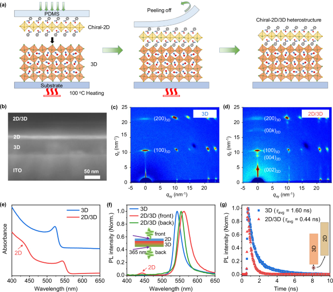
a Schematic diagram illustrating the transfer-printing method used to prepare chiral-2D/3D perovskite heterostructures. b Cross-sectional SEM image of the 2D/3D perovskite films. GIWAXS patterns of 3D (c) and 2D/3D (d) perovskite films. e Absorption, f photoluminescence (PL) emission, and g time-resolved PL spectra of 3D and 2D/3D perovskite films. Source data are provided as a Source Data file.
To evaluate the quality of the chiral-2D/3D interface following transfer, we conducted optical microscopy and cross-sectional SEM. The photograph and optical microscopy images (Supplementary Fig. 3) demonstrate that the transferred chiral-2D layers are uniform and intact, and feature with clearly defined edges. Cross-sectional SEM images (Fig. 1b) reveal a thin (~10 nm) chiral-2D layer uniformly covered on 3D perovskite layer (~50 nm). Backscattered SEM imaging (COMPO mode) further differentiates the individual layers based on their atomic densities, where darker color refers to materials with light-weight and low-density atoms, while brighter color indicates heavy and high-density atoms29. As shown in Supplementary Fig. 4, the chiral-2D layer appears as a thin and dark layer on top of the 3D layer due to its higher content of low-density organic cations. These optical and SEM images confirm the formation of a smooth and well-integrated interface between the chiral-2D and the 3D layer. Grazing incidence wide-angle X-ray scattering (GIWAXS) was performed to evaluate the crystalline ordering of perovskites. As shown in Fig. 1c, the pure 3D film exhibits intense and sharp Bragg spots, indicating an ordered crystal structure. The pure chiral-2D film (Supplementary Fig. 5) displays strong Bragg spots along the qz direction, corresponding to the (0 0 2k) planes, suggesting that the chiral-2D perovskite is oriented parallel to the substrate11. As shown in Fig. 1d, the diffraction pattern of the chiral-2D/3D film is a combination of the diffraction patterns from both the pure 3D and chiral-2D layers, with no additional peaks detected, indicating the preservation of crystal orientation during the transfer process. This high degree of structural order and high-quality heterostructure interface are critical for minimizing interfacial defects and enabling efficient charge transport.
As shown in Fig. 1e, the chiral-2D/3D film exhibits a weak absorption peak at 435 nm, which is attributed to absorption from the chiral-2D layer. The chiral-2D/3D film also displays a red shift in the absorption edge (shifted from 536 to 560 nm) compared to the pure 3D film. We attribut this shift to halide exchange (Br/I) between the chiral-2D and 3D layers30. Photoluminescence (PL) spectra were recorded by exciting from the front and back surfaces of the 2D/3D films, respectively (Fig. 1f). When exciting from the front side, an extra PL emission peak at 445 nm was observed. The PL excitation (PLE) spectrum of 445 nm emission is consistent with the absorption spectrum of S-MBA2PbBr2.5I1.5 (Supplementary Fig. 6), indicating that this extra emission originates from the chiral-2D layer. Conversely, the back surface excitation shows only emission from the 3D layer, confirming the chiral-2D layer is exclusively located on the top surface of the 3D layer30. Additionally, the time-resolved photoluminescence (TRPL) measurements were carried out to study the charge transfer and separation at the chiral-2D/3D interface (Fig. 1g). The carrier lifetimes (Supplementary Table 1) were fitted from TRPL curves. The chiral-2D/3D film shows a shorter average carrier lifetime (τavg ≈ 0.44 ns) than the pure 3D film (τavg ≈ 1.6 ns), indicating efficient charge separation between the chiral-2D and 3D layers30.
CPL detector fabrication and performance
To evaluate the performance of our CPL detectors, we fabricated devices with a vertically stacked structure of ITO/SnO2/3D perovskite (MAPbBr3)/chiral-2D perovskite (MBA2PbI4)/Spiro-OMeTAD/Ag. Note that the thickness of the chiral-2D layer in detectors is ~10 nm to ensure efficient charge transport, unless otherwise indicated. Figure 2a shows a cross-sectional SEM image of our CPL detector, displaying a smooth interface and tightly bonded contacts between functional layers, which are essential for optimal device performance. The transient photocurrent response (Supplementary Fig. 7) and −3 dB bandwidth (Supplementary Fig. 8) of our chiral-2D/3D detector reveal a rise time (τr) of 81 μs, a fall time (τf) of 72 μs and a bandwidth of ~5 kHz. These performance metrics surpass those of previously reported chiral low-dimensional perovskite-based CPL detectors, which typically exhibit response time on the order of milliseconds and bandwidths of a few hundred Hz (Supplementary Table 2). The faster response of our detector can be attributed to: a) the vertically stacked heterostructure, instead of the lateral geometry used in photoconductor or phototransistor-based detectors; and b) the higher carrier mobility of 3D perovskites than their low-dimensional counterparts. Figure 2e exhibits the repetitive photocurrent switching characteristics of our detectors operating at 0 V under 532 nm laser illumination (8.1 × 10⁻⁴ W cm−2). The D* of the detectors were calculated using the following equation:
$${{D}}^{\ast }=\frac{{R}\sqrt{{A}}}{{{S}}_{{{{\rm{n}}}}}}$$
(2)
where R is the photoresponsivity (71.5 mA W−1), A is the active area (0.045 cm2), and Sn is the noise current at 1 Hz (4.1 × 10⁻¹⁴ A Hz−1/2, Supplementary Fig. 9). The D* was calculated to be ~3.7 × 10¹¹ Jones, outperforming most previously reported self-powered CPL detectors based on chiral low-dimensional perovskites (Supplementary Table 2). Moreover, this high D* of ~3.7 × 10¹¹ Jones was maintained across light intensity levels from 7.79 × 10⁻⁷ to 1.56 × 10⁻³ W cm−2 (Supplementary Fig. 10), translating to a wide linear dynamic range (LDR) of 66 dB. In contrast, most previously reported perovskite-based CPL detectors show a significant decrease in D* by one or two orders of magnitude as light intensity increases.
Fig. 2: Device structure, spectral performance, and mechanistic analysis of chiral-2D/3D-based CPL Detectors.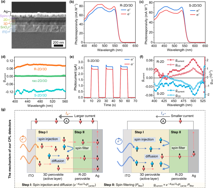
a Cross-sectional SEM image of our CPL detector. Note: The visible cracks in the image are artifacts resulting from the gold coating process used for imaging, and do not affect the integrity of the device layers. Response spectra of the CPL detectors based on R-2D/3D (b) and S-2D/3D (c) perovskite under σ+ and σ− CPL illumination, respectively. d The gcurrent spectra of the detectors based on R-2D/3D, rac-2D/3D, and S-2D/3D perovskite. e The photocurrent differences of S-2D/3D detector under σ+ and σ− CPL illumination (532 nm) at 0 V. f The gCD and gcurrent spectra of the CPL detectors based on pure R-MBA2PbI4 and S-MBA2PbI4. The gCD was calculated using the formula gCD = CD/(32980×absorbance) based on Supplementary Fig. 15. The gcurrent was calculated using Eq. (1), as detailed in Supplementary Fig. 16. g Schematic diagram of the mechanism of chiral-2D/3D-based CPL detectors based on spintronic properties. Source data are provided as a Source Data file.
Next, we measured the photoresponsivity of the CPL detectors based on different combinations of 2D/3D (R-2D/3D, S-2D/3D, rac-2D/3D), pure 3D and R-/S-2D perovskites under σ+ and σ− CPL illumination across a broad wavelength range. To ensure accuracy, the experimental setup was carefully calibrated to minimize artifacts from incident light intensity fluctuations and device degradation (Supplementary Fig. 11). Figure 2b, c illustrate the photoresponsivity spectra of the R-2D/3D and S-2D/3D CPL detectors, respectively. These detectors achieved a peak photoresponsivity of 83.2 mA W−1 at 480 nm, exceeding previous CPL detectors based on low-dimensional perovskites (~1 mA W−1 without bias)20,22,31. Both R-2D/3D and S-2D/3D detectors displayed an asymmetric response within the 400–560 nm range, corresponding to the absorption range of the 3D layer (Fig. 1e). Specifically, R-2D/3D detectors were more sensitive to σ− CPL, while S-2D/3D detectors favored σ+ CPL. Notably, this asymmetric photoresponse diminished when the chiral-2D layer was replaced with achiral rac-MBA2PbI4 (labeled as rac-2D/3D, Supplementary Fig. 12) or when the chiral-2D layer was entirely removed (pure 3D, Supplementary Fig. 13a). To quantify this asymmetry, we calculated the gcurrent values using Eq. (1). Figure 2d and Supplementary Fig. 13b exhibit the gcurrent spectra of the CPL detectors based on R-2D/3D, S-2D/3D, rac-2D/3D and pure 3D perovskite, respectively. Both rac-2D/3D and pure 3D perovskite-based detectors exhibited negligible gcurrent within the detection range. In contrast, R-2D/3D and S-2D/3D detectors maintained nearly constant gcurrent values of ~0.09 and ~−0.11, respectively, across the 400–560 nm range. Furthermore, our chiral-2D/3D heterostructure strategy is adaptable to various chiral-2D perovskites (Supplementary Fig. 14), including R-NEA2PbI4 [R-NEA, R-1-(1-naphthyl)ethylamine], previously utilized in several perovskite CPL detectors, and R-3BrPEA2PbI4 [R-1-(3-bromophenyl)-ethylamine], a new chiral cation not yet explored in such applications. Similar to the MBA-2D/3D heterostructure, these chiral-2D/3D detectors exhibit broad and wavelength-independent gcurrent spectra.
Importantly, this behavior contrasts with the CPL detectors based on pure chiral-2D perovskites, where gcurrent spectra closely follow their CD spectra. As shown in Fig. 2f (extracted from Supplementary Figs. 15 and 16), both gCD and gcurrent spectra of the pure chiral-2D CPL detectors exhibited strong wavelength dependence, with a maximum gcurrent (~0.06) at the excitonic absorption peak (504 nm). Moreover, the negligible CD signals from the chiral-2D/3D films (Supplementary Fig. 17) indicate that the thin chiral-2D layer does not contribute to CPL detection through asymmetric absorption of σ+ and σ− CPL. The wavelength-independent gcurrent of the chiral-2D/3D-based CPL detectors, combined with the negligible CD signal in the chiral-2D/3D films, strongly suggests that the gcurrent in chiral-2D/3D CPL detectors arise from a fundamentally different mechanism compared to conventional chiral-2D based CPL detectors.
Mechanism of CPL detection
As shown in Supplementary Fig. 18, conventional CPL detectors based on chiral materials typically operate by selectively absorbing σ+ and σ− CPL \((\varDelta {A}={{A}}_{{{{{\rm{\sigma }}}}}^{-}}-{{A}}_{{{{{\rm{\sigma }}}}}^{+}})\), leading to a difference in photogenerated carriers \((\varDelta {n}={{n}}_{{{{{\rm{\sigma }}}}}^{-}}-{{n}}_{{{{{\rm{\sigma }}}}}^{+}})\) and eventually an anisotropic photocurrent \((\varDelta {I}={{I}}_{{{{{\rm{\sigma }}}}}^{-}}-{{I}}_{{{{{\rm{\sigma }}}}}^{+}})\). Consequently, the gcurrent value is directly proportional to gCD, following the relationship: \({{g}}_{{{{\rm{current}}}}}=2\varDelta {I}/{I}\propto 2\varDelta {n}/{n}\,=2\varDelta {A}/{A}={{g}}_{{{{\rm{CD}}}}}\). Thus, both gCD and gcurrent spectra of these CPL detectors exhibit a similar wavelength-dependent photoresponse. However, this mechanism fails to explain the large discrepancy observed between the gCD and the gcurrent values in chiral perovskite-based CPL detectors, as well as the wavelength-independent gcurrent observed in our chiral-2D/3D CPL detectors. Therefore, we propose a new mechanism for our chiral-2D/3D CPL detectors, illustrated in Fig. 2g. This mechanism involves two critical steps: (I) optical spin injection in the 3D layer and (II) spin filtering effect in the chiral-2D layer.
Step I: optical spin injection in 3D layer
The first step toward effectively identifying CPL in our detectors is to generate asymmetrical populations of spin-up and spin-down polarized carriers within the 3D layer. Generally, metal halide perovskites (MHPs) incorporating heavy atoms like Pb and halogens (I, Br, etc.) possess strong SOC, which significantly enhances their spin-polarization capability. In the case of MHPs that have non-centrosymmetric space group or undergo lattice distortions, this absence of spatial inversion symmetry and strong SOC leads to Rashba splitting32,33,34. Rashba splitting lifts the band degeneracy, splitting continuum bands into two sub-bands with opposite spin orientations (spin-up or spin-down)26,35. As shown in Fig. 3a, the non-degenerated states at the top of valence band possess angular momentum S = ± 1/2, while the states at the bottom of conduction band have spin angular momentum J = ± 1/2. The optical excitation between these bands obeys the total angular momentum conservation rule, and the corresponding angular momentum change (ΔmJ) is ±1 upon the helicity of the incident light35. Incident CPL transfer their carried angular momentum to the electron orbital momentum of the perovskite. Through SOC interaction, the electron orbital momentum is transferred to the electron spin momentum, generating spin-polarized carriers. Specifically, σ+ CPL selectively generates spin-down carriers, while σ− CPL light induces spin-up carriers36, creating an imbalance in the population of spin-polarized carriers, a phenomenon known as optical spin injection. Notably, Rashba splitting has been observed in various MHPs, such as MAPbBr3, MAPbI3, CsPbBr3, PEA2PbI4, and (AMP)PbI428,37,38,39. For example, Niesner et al. reported a giant Rashba splitting energy (ΔE = 240 meV) in MAPbBr3 at room temperature by directly measuring its valence band using angle-resolved photoelectron spectroscopy (ARPES)28. This much larger ΔE than the thermal activation energy (~26 meV) at room temperature is the prerequisite for spin-related properties such as spin dependent carrier generation and transport, which will be discussed later. Thus, we chose 3D perovskite MAPbBr3 as the active layer for our CPL detectors, taking advantage of its strong SOC and giant Rashba splitting to ensure efficient spin polarization of the carriers.
Fig. 3: Optical spin injection.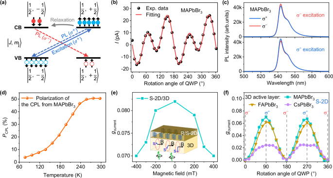
a Schematic diagram for spin-dependent optical transition. b Photogalvanic current as a function of the rotation angle of QWP (α), measured at room temperature. The black dots are measured data. The red solid line is the fitting line using Eq. (4). c The σ+ and σ− CPL emission spectra of MAPbBr3 film under σ+ CPL and σ− CPL (top) excitation at 77 K. d Degree of circular polarization of CPL as a function of temperature for MAPbBr3 film. e The gcurrent value as a function of magnetic field intensity. The inset shows the carrier spin processes around the B direction. f The gcurrent value as a function of the rotation angle of QWP for S-2D/3D perovskite with the active layers of MAPbBr3, FAPbBr3 and CsPbBr3, respectively, under 532 nm irradiance. In the experimental setup, as illustrated in Supplementary Fig. 22, the initial angle between the fast axis of the QWP and the polarization direction of the incident linearly polarized light is set as 45°, not as 0°. This initial configuration directs σ− CPL onto the S-2D/3D detector. Source data are provided as a Source Data file.
To further validate the presence of Rashba splitting in our 3D layer, we performed circular photogalvanic effect (CPGE) and CPL emission measurements (details in Supplementary Figs. 19 and 20), which are crucial indicators for verifying Rashba splitting26,37,38. As illustrated in Supplementary Fig. 19a, Rashba splitting causes the energy bands in k-space to split into two sub-bands with opposite spin orientations. Under σ+ and σ− CPL excitation, carriers are selectively generated in these spin-split sub-bands, acquiring opposite net group velocities in k-space. This will result in photocurrents with opposing directions, depending on the helicity of the incident CPL. The inversion of the photocurrent direction as a function of the incident light helicity provides direct evidence of Rashba splitting in the 3D perovskite films. Figure 3b shows the changes in photocurrent with different QWP angles, which can be described by Eq. (3) and summarized in Supplementary Table 339
$${I}={C}\,\sin (2{{{\rm{\alpha }}}})+{L}\,\sin (4{{{\rm{\alpha }}}}+{{{\rm{\theta }}}})+{D}$$
(3)
where D represents the polarization-independent photocurrent originating from the photovoltaic and damper effects. The coefficients C and L correspond to the magnitudes of the CPGE photocurrent and linear photogalvanic effect photocurrent, respectively. A nonzero C confirms the existence of Rashba splitting and the generation of spin-polarized carriers under CPL irradiation in the 3D layer37,38. Moreover, CPL emission measurements verified the spin-dependent recombination, where the transition occurs between Rashba-induced spin-polarized bands, as illustrated in Fig. 3a. When spin-polarized carriers undergo radiative recombination, they emit CPL with opposite helicity (σ+ or σ−) depending on their spin states. The degree of circular polarization for the CPL (PCPL) is proportional to the degree of spin polarization of the carriers (Pcarrier)26. Given this reciprocal relationship between spin-dependent excitation and emission, the Pcarrier in the 3D layer can be reflected by the PCPL of the 3D layer26:
$${{P}}_{{{{\rm{carrier}}}}}=\left|\frac{{{N}}_{\uparrow }-{{N}}_{\downarrow }}{{{N}}_{\uparrow }+{{N}}_{\downarrow }}\right|\approx \left|\frac{{{L}}_{{\sigma }^{-}}-{{L}}_{{\sigma }^{+}}}{{{L}}_{{\sigma }^{-}}+{{L}}_{{\sigma }^{+}}}\right|={{P}}_{{{{\rm{CPL}}}}}$$
(4)
where N↑ and N↓ represent the populations of spin-up and spin-down carriers, respectively, and \({{L}}_{{\sigma }^{+}}\) and \({{L}}_{{\sigma }^{-}}\) represent the maximum light intensity of σ+ and σ− CPL, respectively. The PCPL was measured by exciting the 3D layer with a linearly polarized laser (487 nm) that passed through a QWP, as detailed in Supplementary Fig. 20. By rotating the QWP to 45° and 135°, the linear polarization was transformed into σ+ and σ− CPL, respectively. Figure 3c presents the CPL spectra of the 3D layer measured at 77 K under σ+ and σ− CPL excitation, respectively. As shown in Fig. 3d and Supplementary Fig. 21, the PCPL in 3D layer was ~3.8% at 77 K and increased to 50.5% at room temperature. This significant rise in PCPL with increasing temperature can be attributed to dynamically thermally assisted Rashba splitting39,40. As temperature increases, the organic cations (MA+) in MAPbBr3 undergo more vigorous rotation, breaking the local inversion asymmetry and further enhancing the Rashba splitting40. Note such a high PCPL (~50.5%) is achieved at room temperature without an external magnetic field or ferromagnetic electrodes, confirming the efficient generation of spin-polarized carriers in the 3D layer through optical spin injection.
Subsequently, the imbalanced spin-polarized carriers generated by CPL excitation migrate toward the chiral-2D/3D interface and contribute to an asymmetry in the photocurrent (gcurrent, Fig. 2g). Essentially, the gcurrent values in our detectors are proportional to Pcarrier, thereby allowing us to modulate gcurrent values by controlling Pcarrier. To verify the spin-polarized charge carriers in 3D perovskite contribute to CPL detection, we applied an external magnetic field (By) perpendicular to the spin orientation of carriers, as shown in the inset of Fig. 3e. This magnetic field induces Larmor precession of the spin-polarized carriers around the By direction, resulting in a quenching of Pcarrier, a phenomenon known as a Hanle effect26,27. Figure 3e shows that the gcurrent of the chiral-2D/3D CPL detector decreases with increasing By, unambiguously indicating that the gcurrent in our detector is correlated with spin-polarized carriers in the 3D layer. On the other hand, spin relaxation processes inherently occur during transport in the 3D layer. Herein, three widely-used 3D perovskites: MAPbBr3, FAPbBr3 and CsPbBr3 were tested as 3D layers due to their varying degrees of Rashba splitting and spin relaxation times. A large Rashba splitting is generally advantageous for suppressing spin relaxation and enhancing spin polarization. Figure 3f presents the gcurrent values under varying QWP rotation angles for the chiral-2D/3D CPL detectors based on S-2D/MAPbBr3, S-2D/FAPbBr3 and S-2D/CsPbBr3 (details in Supplementary Fig. 22). The gcurrent values follow the trend: S-2D/MAPbBr3 (~0.07) > S-2D/FAPbBr3 (~0.06) > S-2D/CsPbBr3 (~0.02). This trend aligns with the degree of Rashba splitting and spin relaxation times in these 3D perovskites: MAPbBr3 > FAPbBr3 > CsPbBr327,41,42. Furthermore, we measured the gcurrent values of S-2D/MAPbBr3 as a function of the thickness of 3D layer. As depicted in Supplementary Fig. 23, \({g}_{{{{\rm{current}}}}}\) values follow an exponential decay with increasing 3D layer thickness (d3D), \({g}_{{\rm{current}}}={g}_{0}{{\rm{e}}}^{-{d}_{3{{\rm{D}}}}/{{\rm{\lambda }}}_{{\rm{s}}}}\)43,44. This trend implies that the spin-polarized carriers diffuse through the 3D layer43, and the spin diffusion length (λs) of 3D layer significantly impacts the gcurrent. By applying the exponential decay model, the λs in the MAPbBr3 layer was estimated to be ~85 nm, close to the reported values44,45. Consequently, these findings confirm that the gcurrent values in chiral-2D/3D CPL detectors are indeed linked with the spin polarization of photogenerated carriers and spin relaxation processes in the 3D layer, following the relationship: \({g}_{{{{\rm{current}}}}}\propto {{{{\rm{e}}}}}^{-{d}_{{{{\rm{3D}}}}}{/{{{\rm{\lambda }}}}}_{{{{\rm{s}}}}}}{P}_{{{{\rm{carrier}}}}}\)
Step 2: Spin filtering in chiral-2D layer
The second step in our CPL detection paradigm involves spin filtering the generated spin-polarized charge carriers by the chiral-2D layer. As these carriers migrate into the chiral-2D layer, they undergo selective transport depending on their spin orientations. Note, this selective transport in the chiral-2D layer is wavelength-independent, which is pivotal for achieving panchromatic CPL detection. Without the chiral-2D layer, a non-ferromagnetic (Ag) electrode would indiscriminately collect all spin-polarized carriers, displaying identical photocurrent and nondiscrimination for incident CPLs. Chiral-2D perovskites typically adopt a horizontal orientation, wherein their chiral organic ligands align perpendicularly to the substrate, creating vertical helical potentials35. As illustrated in Fig. 4a, as carriers move through the helical potentials, they induce an effective magnetic field, analogous to a classical electromagnetic coil46. The direction of induced effective magnetic field is determined by the helix’s chirality and significantly impacts the transport dynamics of the carriers. Specifically, carriers whose spin direction aligns with the effective magnetic field are preferentially transported, while carriers with opposite spin are hindered. This selective transport mechanism, known as the chirality-induced spin selectivity (CISS) effect, was further investigated by using magnetic conductive-probe AFM (mCP-AFM) (Supplementary Fig. 24)11,35. Spin-polarized currents were injected into the chiral-2D layers using ferromagnetic (Co/Cr coated) AFM tips, magnetized either “up” or “down” via an external magnetic field. Figure 4b, c (details in Supplementary Fig. 25) shows the averaged current-voltage (I-V) curves for R-2D and S-2D layers (~107 nm), respectively. For the R-2D layer, a higher current was observed with “up” magnetization than “down” magnetization, indicating that the R-2D layer facilitates the transport of spin-up carriers while filtering out spin-down carriers. Conversely, the S-2D layer preferred spin-down carriers. The spin filtering efficiency (Pfilter) is quantitatively determined by11:
$${{P}}_{{{{\rm{filter}}}}}=\frac{{{I}}_{{{{\rm{up}}}}}-{{I}}_{{{{\rm{down}}}}}}{{{I}}_{{{{\rm{up}}}}}+{{I}}_{{{{\rm{down}}}}}}$$
(5)
where Iup and Idown are the average spin-polarized currents for “up” and “down” magnetized tips, respectively. Pfilter values for R-MBA2PbI4 and S-MBA2PbI4 films were as high as +82% and −79%, respectively. Considering that mc-AFM measurement provides only the local Pfilter, we further explored the CISS effect of the chiral-2D layer in a large area identical to our CPL detector. We fabricated half-spin valve devices (area = 4.5 mm2) with a structure of ferronickel (NiFe)/Aluminum oxide (Al2O3)/R-/S-MBA2PbI4/bathocuproine (BCP)/molybdenum trioxide (MoO3)/Al35. NiFe electrodes were used to electrically inject spin-polarized charge carriers into the chiral-2D layer, resulting in chirality-dependent current asymmetry (Supplementary Fig. 26). The current was higher for R-2D device when the NiFe magnetization was “up” than “down”, whereas the S-2D device exhibited an opposite trend. The corresponding Pfilter values for the devices based on R-2D layer and S-2D layer were +36% and −41%, respectively. This lower Pfilter compared to mCP-AFM results might be due to the pinhole-induced leakage currents47. Nevertheless, these significant Pfilter values unambiguously confirm the CISS effect of R/S-2D layers. Similarly, R-2D/3D and S-2D/3D heterostructure films exhibited Pfilter values of +18% and −23%, respectively (Supplementary Fig. 27), lower than pure R-2D and S-2D layers. This decrease in Pfilter of chiral-2D/3D films is attributed to the reduced thickness of the chiral-2D layers (~10 nm vs 107 nm)48.
Fig. 4: Spin filtering.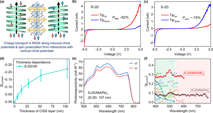
a Schematic illustration of the origin of the CISS effect. Charge carrier transport along vertically induced chiral (helical) potentials results in spin filtering. Current versus voltage (I-V) curves measured by mCP-AFM technique for R-MBA2PbI4 (b) and S-MBA2PbI4 (c) films. The probe was magnetized in the up (red) and down (blue) orientations. The I-V curve for each film was averaged 10 scans at different points (raw data presented in Supplementary Fig. 25). d The gcurrent as a function of the thickness of the S-2D layer for S-2D/3D CPL detectors. Error bars represent the standard deviation from five independent devices. e Response spectra of the S-2D/MAPbI3 detector with ~107 nm S-2D layer under σ+ and σ− CPL illumination. f The gcurrent spectra of our chiral-2D/3D CPL detector and the reference CPL detectors, as detailed in Supplementary Table 2. The green region indicates the typical detection range of most reported chiral perovskite-based CPL detectors. The red region represents the extended detection range rarely covered by chiral perovskite-based CPL detectors. Source data are provided as a Source Data file.
In our chiral-2D/3D CPL detectors, as illustrated in Fig. 2g, selective spin filtration through the chiral-2D layer creates an imbalance in the populations of “up” and “down” spin-polarized carriers collected by Ag electrodes, resulting in asymmetric photocurrents for σ+ and σ− CPL \(\varDelta {I}{=}{I}_{{\sigma }^{-}}-{I}_{{{{{\rm{\sigma }}}}}^{+}}\). Consequently, the final gcurrent value of chiral-2D/3D CPL detector is determined by both the polarization degree of the carriers in the 3D layer (Pcarrier) and the CISS efficiency of the chiral-2D perovskite filter layer (Pfilter), which can be expressed as below:
$${{g}}_{{{{\rm{current}}}}}=2\frac{\varDelta {I}}{{I}}\approx {{{{\rm{2e}}}}}^{-{d}_{{{{\rm{3D}}}}}{/{{{\rm{\lambda }}}}}_{{{{\rm{s}}}}}}\frac{{{N}}_{\uparrow }-{{N}}_{\downarrow }}{{{N}}_{\uparrow }+{{N}}_{\downarrow }}{{P}}_{{{{\rm{filter}}}}}{={{{\rm{2e}}}}}^{-{d}_{{{{\rm{3D}}}}}{/{{{\rm{\lambda }}}}}_{{{{\rm{s}}}}}}{{P}}_{{{{\rm{carrier}}}}}{{P}}_{{{{\rm{filter}}}}}$$
(6)
It is evident that gcurrent can be modulated by adjusting the thickness of the chiral-2D layer, since thickness directly impacts Pfilter48. However, increasing the chiral-2D layer thickness also amplifies its CD absorption (Supplementary Fig. 28). To exclude the contribution from the CD absorption of the chiral-2D layers, we used 532 nm light, which excites only 3D layers but not chiral 2D layers, to study the thickness-dependent gcurrent. Notably, while thicker chiral-2D layers typically increase Pfilter, they also introduce a spin relaxation process due to enhanced spin scattering. This competition between spin filtration and spin relaxation results in a nonlinear relationship between gcurrent (Pfilter) and the thickness of the chiral-2D layer11. Specifically, the gcurrent increases rapidly with the thickness of the chiral-2D layer, eventually saturating around 50 nm (Fig. 4d). As shown in Supplementary Fig. 29 and Fig. 4f, incorporating a thicker (~107 nm) chiral-2D layer enhances the Pfilter and leads to a higher average gcurrent value of 0.28 across the broad range (400–600 nm) and maximum 0.35 at 495 nm. The average gcurrent matches the theoretically predicted value (~0.23) from Eq. (6), considering carrier polarization and spin filtering effects. For CPL detection at 495 nm, the gcurrent should also incorporate the contribution of chiroptical absorption of the thick chiral-2D perovskite layer, described as: \({{g}}_{{{{\rm{current}}}}}\approx {{{{\rm{2e}}}}}^{-{d}_{{{{\rm{3D}}}}}{/{{{\rm{\lambda }}}}}_{{{{\rm{s}}}}}}{{P}}_{{{{\rm{carrier}}}}}{{P}}_{{{{\rm{filter}}}}}+{{g}}_{{{{\rm{CD}}}}}\).
Figure 4f summarizes the gcurrent values of our chiral-2D/3D CPL detectors in comparison with previously reported CPL detectors based on chiral low-dimensional perovskites. The gcurrent values of our detectors surpass those of most previously reported devices, which typically show gcurrent values below 0.2. Notably, conventional CPL detectors usually exhibit a CPL response within a narrow spectral range of only a few tens of nanometers, with their detection capability typically limited to wavelengths below 520 nm. In contrast, our detectors achieve a panchromatic CPL response across the visible spectrum, with the detection range determined by the bandgap of the 3D layer materials. As shown in Figs. 4e, f, replacing the 3D MAPbBr3 layer with a lower bandgap 3D MAPbI3 layer further extends the CPL detection range up to 760 nm, although the gcurrent value decreases to ~0.1 possibly due to the shorter spin relaxation time of the MAPbI3 layer. Nonetheless, our strategy provides the flexibility to broaden the CPL detection spectrum by selecting appropriate active layer materials.