The first Nvidia Blackwell GPU wafer emerged this week from the TSMC chip fabrication plant in Phoenix, Arizona, marking a milestone in advanced semiconductor manufacturing on US soil.
“This is a historic moment for several reasons,” stated Nvidia CEO Jensen Huang in a ceremony at the TSMC Arizona fab. “It’s the very first time in recent American history that the single most important chip is being manufactured here in the United States by the most advanced fab, by TSMC, here in the United States.
“This is the vision of President Trump of reindustrialization–to bring back manufacturing to America, to create jobs, of course, but also, this is the single most vital manufacturing industry and the most important technology industry in the world,” Huang continued.
Amid the AI boom, Nvidia has struggled to keep up with demand for its data center GPUs, in particular the Blackwell, its fastest and most powerful chip for AI and HPC workloads. Up to this point, Blackwell production has occurred only at Taiwan Semiconductor Manufacturing Company (TMSC)’s fab in Taiwan. The establishment of Blackwell production in Phoenix is good news for Nvidia and TSMC, as well as AI customers.
 Nvidia and TSMC executives celebrating the first Blackwell wafer from the TSMC Arizona fab
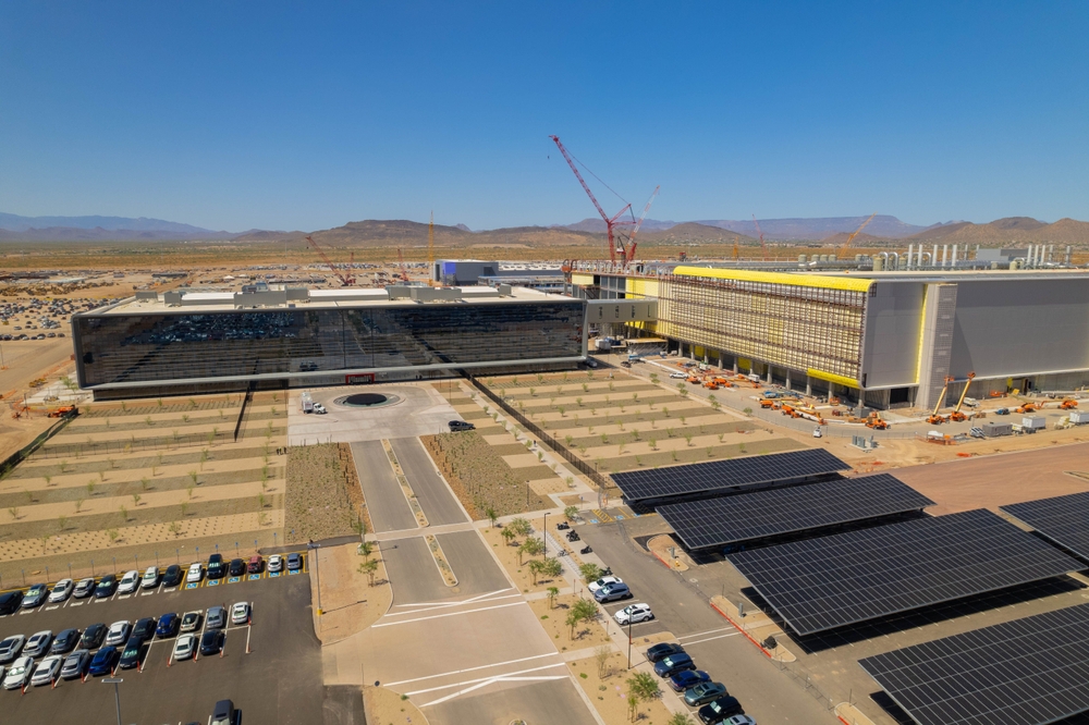
The Phoenix plant was first conceived in 2020, when TSMC announced it would build Fab 21 in the empty lands of northwest Phoenix. The goal was to bring to the facility its newest 5nm process (the one currently used to create Blackwell wafers) and manufacture up to 20,000 wafers per month when the fab finally went into production in 2024, followed by additional fabs with its 3nm and 2nm processes. All told, the chip giant planned to spend $12 billion on the project over eight years.
As the COVID pandemic ground on and the chip shortage became more acute, the total construction cost went up 3x. TSMC increased its investment, and it also got help from the US Government, which pledged to provide up to $6.6 billion in direct funding and $5 billion in loans through the CHIPS and Science Act.
At this point, the total investment in the TSMC Arizona facility is slated to total $165 billion, with six fabs in total built on the grounds of the facility. In addition to the 3nm and 2nm fabs, which are slated to go into production in 2029, it also is planning to manufacture chips using its newest 1.6nm process.
“To go from arriving in Arizona to delivering the first U.S.-made NVIDIA Blackwell chip in just a few short years represents the very best of TSMC,” TSMC Arizona CEO Ray Chuang stated. “This milestone is built on three decades of partnership with NVIDIA — pushing the boundaries of technology together — and on the unwavering dedication of our employees and the local partners who helped to make TSMC Arizona possible.”
The creation of the Blackwell wafer is just the first step in a GPU’s journey. Ultimately, some of these chips will be placed in a full GB200 NVL72 system. For a fascinating video on the steps that are involved in the manufacturing process, check out the video below.