By “virtually” combining two FeFET devices into a single structure, as depicted in Fig. 2, the storage capacity of a FeFET-based crossbar array is effectively doubled. Figure 2B illustrates the detailed structure of our proposed design, featuring two distinct gate contacts: the upper gate (U-Gate) and the lower gate (L-Gate), respectively.
Fig. 2: When deployed in Edge Inferencing, conventional FeFET based arrays suffer from the need to frequently reprogram the cells with new weights, which quickly downgrades the device endurance.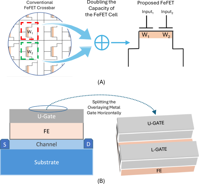
A The proposed FeFET device can store two weights inside the same cell locally and independently, doubling the array’s capacity and improving endurance. B That is achieved by splitting the metal gate along the source-drain axis, enabling local polarization of the FE layer.
Split-gate device operation
The split-gate structure enables localized polarization of the FE layer directly beneath each respective gate contact. Figure 3A presents a cross-sectional view of the gate stack, oriented perpendicular to the source-drain axis. When programming voltages are applied to both gate contacts (for instance, positive voltages to induce downward polarization in both regions), the two regions of the FE layer under each gate are polarized independently. A downward polarization (PFE+) results in a low-threshold voltage (LVT) state, characterized by high channel conductance, representing logic “1”. Conversely, an upward polarization (PFE−) corresponds to a high-threshold voltage (HVT) state, with low conductance, representing logic “0”.
Fig. 3: Structure and operation of the proposed split-gate FeFET.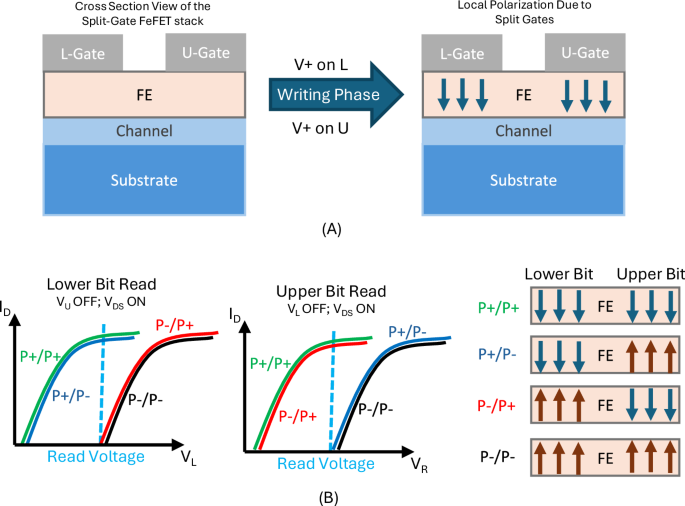
A The split gates enable independent writing of dual bits into the device. A large positive pulse on one of the gates would positively polarize the FE area under it, which programs the corresponding bit with the logic value “1”. Similarly, A large negative pulse would result in logic “0”. B Reading schemes for accessing the lower and upper bits stored in the device in addition to the four possible combinations of stored bits and their corresponding polarization states. Unlike the conventional MLC, the two bits cannot be read in the same cycle since they require different biases. However, under this scheme, the FE cell can hold four combinations of two locally and independently stored bits.
During the write phase, the appropriate write voltage is applied to the targeted gate contact, selectively polarizing the underlying FE material and programming the desired bit. The localized polarization ensures that each bit is independently stored in its respective region of the FE layer. The read operation, as depicted in Fig. 3B, involves applying a specific read bias depending on the desired bit to access the stored information.
To represent the state of the entire split-gate device, we use the notation [Pol. L-Gate ∣ Pol. U-Gate], where the polarization of the lower and upper gates is explicitly noted. For example, storing logic “1” in both regions is denoted as [PFE+∣PFE+]. Figure 3B illustrates all four possible combinations of stored bits and their corresponding ideal read operations. For instance, when reading the lower bit, the U-Gate voltage is set to VU-Gate = VOFF and the L-Gate voltage is set to VL-Gate = Vread. Consequently, the drain current is primarily determined by the polarization state of the L-Gate region. The current will be high if the lower gate stores logic “1” (i.e., [PFE+∣X]) and low if it stores logic “0” (i.e., [PFE−∣X]).
Read scheme validation
Figure 4A illustrates the device structure simulated in TCAD20, where the voltage biases employed are Vread = 0 V and VOFF = − 1.2 V. The baseline device is a 14 nm Fully-Depleted Silicon on Insulator (FDSOI) logic transistor, modified by incorporating a 10 nm thick FE layer to create a FeFET. The channel dimensions are 100 nm in both width and length, while each gate contact spans 45 nm, with a 10 nm gap separating the contacts. The ID − VG sweeps for reading the lower bit are shown in Fig. 4B, displaying the characteristics for all four possible polarization states. The device achieves leakage currents lower than 1e–10 A across all cases, while the on-state current exceeds 1e–5 A when storing a logic “1”. The read margin between the [PFE+∣PFE−] and [PFE−∣PFE+] states shows a separation of more than seven orders of magnitude in the measured current, indicating excellent read fidelity. As we simulate an ideal and symmetric device, the results for reading the upper bit, as seen in Fig. 4C, are mirrored accordingly. Figure 5 provides the electron density distribution in the channel during the read operation. Since electron density directly affects channel conductivity, it serves as a reliable indicator of the expected current. The electron density maps further confirm the localized operation of the split-gate architecture. The top left and bottom right maps depict the scenarios where the current is suppressed due to the “0” state being read, even when the other region stores a “1”. The applied VOFF at the gate of the non-targeted bit suppresses the channel formation, ensuring low total drain currents. In contrast, the bottom left and top right maps correspond to high total drain currents, where a “1” bit is being read, and the elevated electron density under the gate forms a conductive channel.
Fig. 4: To validate the split-gate dual-bit concept, TCAD simulations were used.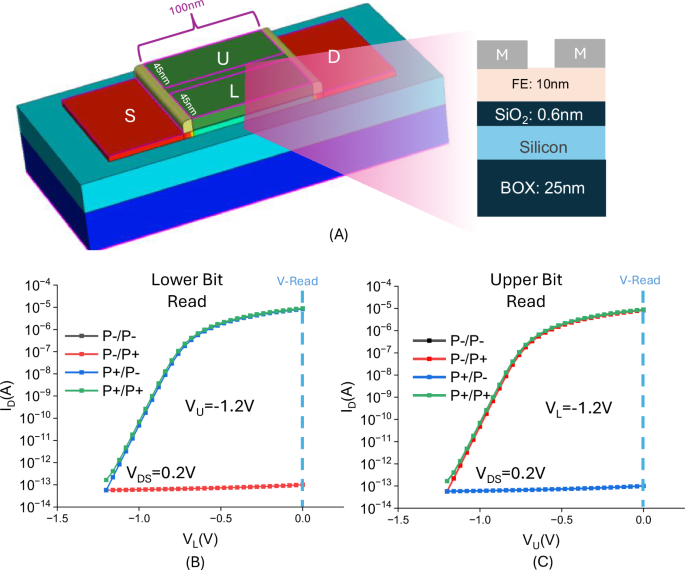
A Shows a 100 nm × 100 nm split-gate device asseen in TCAD with each gate contact covering 45% of the total channel width. It is important to keep the size of the middle part of the FE layer that has no overlaying gate as small as 10 nm width to avoid unwanted current flow. B Simulation results for reading the lower bit. C Simulation results for reading the upper bit. Read simulations showcase a mirrored behavior for the two reading cases, simplifying the overhead required to infer the stored values. In the idle case, the channel is suppressed with −1.2 V on bothsplit-gates. When reading one of the two bits, that suppression voltage islifted from the respective gate.
Fig. 5: Further illustration of the reading scheme and the Independence of the two bits using electron density maps of the channel for the two cases [PFE+∣PFE−] and [PFE−∣PFE+].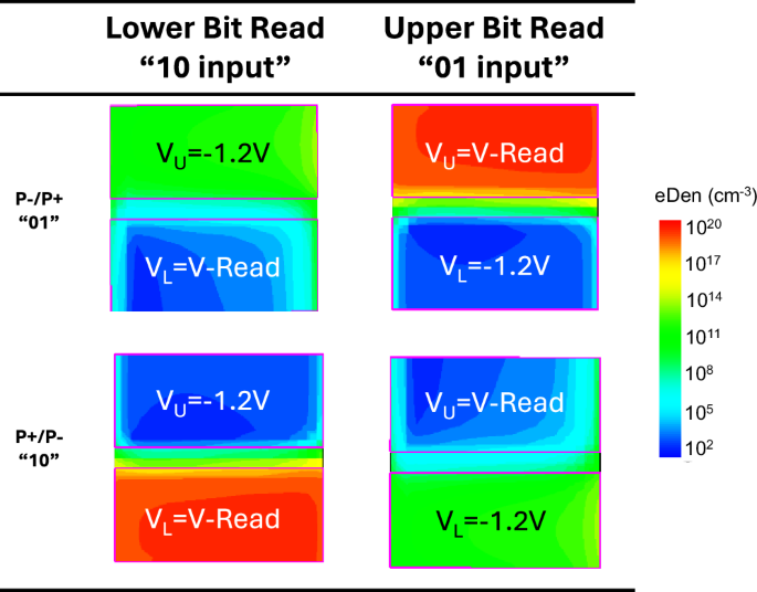
Despite the positive polarization in the upper FE area of the [PFE−∣PFE+], we observe a low electron density in the channel when a −1.2 V is applied on the upper gate. These maps demonstrate the “and” operation that happens independently between the polarization of each FE section and the input on the respective gate. High electron density is only observed when the input on a given gate is logic “1”, and the FE area underneath that gate is polarized positively.
Write scheme validation
The write operation for the proposed dual-bit FeFET is validated using a device with dimensions identical to those discussed in the read validation. However, the FE layer is structured as a 20 × 20 array of smaller FE domains. Figure 6A illustrates the initial configuration of the FE layer, where domains are randomly polarized in either the PFE+ (blue) or PFE− (brown) state. This initialization is achieved by introducing a fixed charge concentration at the interface between the domains and the SiO2 layer.
Fig. 6: Our TCAD domain-based framework was used to validate the writing process.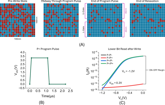
A The switching development is presented throughout the writing phase, while two +3.3 V pulses are applied to each gate simultaneously. The FE layer is first initialized randomly with a 50% split of PFE+ (Blue) and PFE− (Brown) domains. B The programming pulse used on both gates consists of writing and relaxation phases. C Results of reading the lower bit after writing the device with all 2-bit combinations. Despite partial switching, the reading margin between the ON and OFF states is still large.
The programming pulse of 3.3 V (or the erase pulse of −3.3 V), as shown in Fig. 6B, is applied to the selected gate to program a logic “1” (or “0”) in the localized FE region beneath the gate. The vertical electric field generated by the applied pulse induces switching within the FE domains based on the input voltage. To ensure sufficient domain switching, the pulse duration is set to 1 μs, allowing adequate time for the majority of domains to flip. A single write cycle can program both gates simultaneously, as the switching of domains in one region has minimal impact on the other side of the FE layer. In Fig. 6A, the domain-switching pattern during the application of two programming pulses is depicted. By the end of the pulses, most negatively polarized domains have switched, transforming the upper and lower regions of the FE layer into low-threshold voltage states.
To confirm the stability of the polarization, the write pulse is followed by a relaxation phase with VL-Gate = VU-Gate = 0.0 V for 1 μs. The domain configuration remains unchanged after this relaxation period, demonstrating that the switching is neither transient nor spontaneous.
Although the 3.3 V pulse does not switch every domain to the desired state, a substantial on-state/off-state margin is still observed in Fig. 6C. The four curves correspond to reading the device after programming each of the four possible PFE combinations. While increasing the pulse amplitude could improve domain switching uniformity, this would come at the cost of reduced endurance due to the accelerated fatigue of the FE material. Therefore, a balance is struck between sufficient on/off margin and long-term device reliability.
Analyzing the effects of variation
As previously outlined, our proposed dual-bit FeFET design transitions from partial polarization across the entire FE layer, which is a characteristic of MLC operation, to localized full polarization within targeted regions. This localized polarization approach significantly enhances resilience to random spatial variations, a common issue that affects conventional MLC operation, where partial polarization is highly susceptible to variability. By storing discrete binary states with full polarization, the design mitigates the effects of variation on device performance.
To validate this resilience, we tested the read operation on FeFET devices incorporating non-ideal post-program/erase configurations. FeFET devices are not only affected by variations in domain switching but are also subject to conventional sources of variation typical in traditional CMOS transistors. For the conventional variation sources of the underlying CMOS transistor, random dopant fluctuation, metal work-function variation, and line edge roughness were considered21. In addition, variations occurring due to the random location of polarized domains in a multi-domain FE layer are considered. By employing the baseline variation data for low VTH and high VTH states in FeFET devices from21, which accounts for conventional sources of variation, the total variance of the device can be obtained by combining it with the domain switching variance. This combination is valid under the assumption that the two variation sources are independent21. In this model, the different VTH states are abstracted based on FE grid domain configurations, where variations in domain switching translate directly into changes in the VTH state.
Our read scheme was rigorously tested on randomly generated FE grid configurations with a 5% switching variance from the two ideal states: [PFE−∣PFE+] and [PFE+∣PFE−]. These corner states were selected as they represent the most challenging cases due to their proximity, while the near-full polarization states are more easily distinguishable. Figure 7A shows the VTH distributions of the L-Gate across 1000 randomly generated samples, incorporating both conventional sources of variation and a 5% domain switching variance. Despite this combined variation, the resulting distributions maintain a large memory window between the high VTH and low VTH states in the lower FE region. The lower-bit read operation preserves a robust average memory window of 1.61 V. Both VTH states exhibit small standard deviations around 39.55 mV and 25.69 mV, well below the threshold required to disrupt reliable operation. Given the symmetry of the split-gate device, these results can be directly extended to the upper bit. For comparison, Fig. 7B illustrates the VTH distributions for 1000 VTH samples of a conventional FeFET MLC, combining all sources of variation. The results show a much smaller margin between the corner states.
Fig. 7: The effect of variation on the memory window.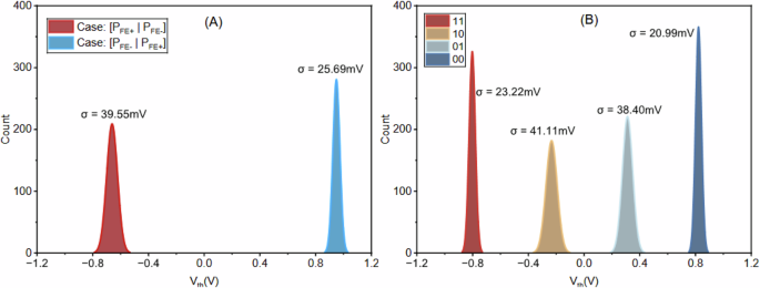
A L-Gate threshold voltage variation due to conventional sources combined with domain switching variance. Despite the variation, the device demonstrated a big margin between the two corner cases: [PFE+∣PFE−] and [PFE−∣PFE+]. Due to the symmetry of the device, U-Gate is expected to behave similarly thanks to the perfect symmetry of the operation and the structure. B The effect of conventional variation sources and domain switching variance on a conventional FeFET based MLC. Unlike our proposed structure, a conventional MLC shows a much smaller separation between logic levels.
In summary, the proposed split-gate FeFET structure demonstrates substantial resilience to variation. This robustness stems from the localized, spatially isolated storage of individual bits, rather than relying on intermediate VTH or ID levels, as in MLC designs. The binary distinction between the two states is based on the presence or absence of channel current, making small VTH variances negligible. Consequently, this architecture allows for reduced write voltages, as full polarization is not required to maintain reliable data storage, as confirmed in the write validation section.