Researchers at Oak Ridge National Laboratory, along with other scientists, are taking small steps to create materials that could enable quantum leaps in computing speed, security in communications and detector sensitivity.
Key tools in this effort to make quantum materials are advanced microscopes, including a recent ORNL development called the “synthescope.” This modified scanning transmission electron microscope (STEM) enables researchers to “write” with atoms, potentially placing them exactly where they are needed within a substance to create a novel material with desirable tailored properties.
A recent breakthrough is the use of artificial intelligence (AI), which learns how to manipulate atoms to improve a material’s properties through precise control of the speed of introducing atoms and the size of electrical pulses used to position the new atoms among the original ones in the target material.
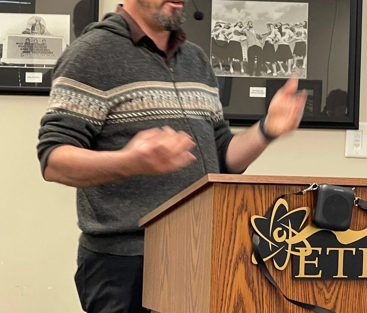
Those were some of the messages of Stephen Jesse, a materials scientist who heads the Nanomaterials Characterizations Section at the Center for Nanophase Materials Sciences (CNMS) at ORNL. He spoke to Friends of ORNL on “Building Materials and Devices with Atomic Precision: Perils and Promise.”
Jesse said he and his colleagues work with atomic force microscopes, scanning tunneling microscopes and STEMs at the atomic scale where quantum properties emerge and persist. This new class of data carriers, including polarized photons of light, trapped atomic ions with different energy levels and electronic or atomic spins oriented up or down, can be used as “qubits.” Qubits are the quantum version of the bits in traditional computers.
They encode quantum information, as in quantum computers and other technologies, the basis for the world’s second quantum revolution. One goal is to make quantum materials that will allow the construction of working quantum computers that would be faster and more powerful than digital supercomputers such as Frontier at ORNL, but would likely supplement them, not replace them.
Jesse provided a quick explanation of quantum information science, which dozens of ORNL researchers work on. The United Nations has declared 2025 the International Year of Quantum Science and Technology, when nations compete to achieve quantum supremacy.
Digital supercomputers have trillions of switches in the form of tiny transistors, he said. Each transistor works like a light switch; it’s either off or on (0 or 1), and a bit is a unit of information expressed as either a 0 or 1 in binary notation. Some have predicted a quantum computer is expected to need only 50 or 60 well-performing qubits, each made of a few atoms, to approach the computational power of much larger digital computers, Jesse remarked.
A qubit is a unit of information more like a dimmer switch, except it can be in many positions at the same time, including off and on (0 and 1) simultaneously. Qubits can exist in multiple states at once – a phenomenon unique to quantum mechanics, which is known as superposition – while a bit can be in only one state at a time, either on or off. The transistor either lets an electrical signal pass through or blocks it.
Quantum computations will be able to explore a vast number of possibilities simultaneously, potentially solving certain problems much faster than classical digital computers, such as designing a new medicine or breaking into a secret code by factoring a huge number. One problem with qubits is that they are fragile and extremely sensitive to temperatures, vibrations and other environmental disturbances, making them difficult to control and maintain unless they are cooled to almost absolute zero.
The challenge for Jesse and other researchers at ORNL is to find ways using advanced microscopes to create a novel combination of atoms – say, metal atoms “planted” in a small amount of graphene, which is one layer of carbon atoms arranged in a hexagonal lattice like chicken wire – that can do incredibly rapid quantum computations without losing the fragile information.
The perfect qubit is the goal.
After mentioning that the scanning tunneling microscope (STM) was developed in 1981 and won its inventors a Nobel Prize in Physics in 1986, Jesse noted that in 1989, IBM scientists in San Jose, California, used an STM to manipulate 35 xenon atoms on a cold nickel surface, spelling IBM in letters 5 nanometers tall. In 1993 at the same IBM lab, a quantum corral was made when 48 iron atoms were placed on a cold copper surface in a ring roughly 71 angstroms in diameter.
Jesse mentioned the work of Michelle Simmons and her team at the University of New South Wales in Sydney, Australia, in using STM lithography to precisely position phosphorus atoms among silicon atoms in a material, enabling the construction of atomic-scale devices with quantum computing components.
In one explanation of how a similar process works at ORNL, Jesse said a STEM has been used to shoot an electron beam at a target material, drilling a hole where desired that is only a few atoms wide. Then by heating a material using MEMS heater chips, the scientists “evaporate atoms onto the surface on which they will skate around at the right temperature and fill and bond to that hole.”
He added that the 200,000 electron-volt e-beam “has a pretty big electric field around it, so if atoms of silicon running around have a charge, they will probably be attracted to the drilled holes” in the graphene or other target material.
Jesse reviewed some of the early STM-based atomic fabrication at CNMS published by ORNL’s An-Ping Li and others in 2017 in Nature Communication. The new method synthesizes semiconducting graphene nanoribbons from polymer precursors by injecting electrical charges from an STM’s scanning probe tip on selective molecular sites. The ORNL researchers were able to grow ultra-narrow graphene ribbons without the typically used metal substrate, yielding a wide band gap semiconductor useful for electronics applications.
Albina Borisevich, who is in Jesse’s CNMS section, showed how to use the STEM’s electron beam to induce transformations in a strontium titanate solid that was part crystalline and part amorphous. She was able to crystallize some of the amorphous section by creating a feedback system using a focused electron beam.
Jesse said ORNL scientists like Mina Yoon are modeling, while others are doing experiments, on “writing” with atoms in thin materials. “There’s a lot of potential for using defects in two-dimensional materials to be qubits,” he noted. He indicated that a computer model showed that removing two carbon atoms from a perfect 3D diamond and replacing one atom with a nitrogen atom while leaving a vacancy creates a structure in which “a single extra electron can hop back and forth between different energy bands.”
But 3D materials are hard to work with, so experimentation went forth focusing mostly on graphene and other 2D materials at CNMS.
According to Jesse, Ondrej Dyck at CNMS was able to use STEM in such a way that a silicon atom was attracted as a dopant by the electric field emanating from the microscope’s electron beam, which created a vacancy for the dopant by drilling a hole in a suspended single layer of graphene. His team showed that dopant atoms of silicon were adsorbed onto the graphene surface and that substitutional dopants could be atoms of copper, tin, titanium, chromium, iron, cobalt, nickel, palladium, silver and platinum.
For example, Jesse said, “We were able to do feedback-driven, atomic-scale writing of copper dopants in a bilayer of graphene” – two layers of carbon atoms.
“From this work we concluded that we needed a more robust and general approach to position atoms,” Jesse said, noting that work began on inventing the synthescope, a significant advance in electron microscopy and materials science because it can augment atomic-scale synthesis. The synthescope development is being done in collaboration with two scientists at the Massachusetts Institute of Technology.
“To make the synthescope, we added to the STEM chemical vapor deposition, pulsed laser deposition, heat treatments and characterization to determine transport and to do optical spectroscopy,” Jesse explained, noting that when the electron beam shines on a target material’s defects, photons of light are emitted, enabling measurements with atomic-scale resolution.
“During synthescope development, we synthesized atoms of two-dimensional tin to be positioned as dopants on graphene,” he said. To improve control and temperature, the researchers added pulsed laser deposition, pulsed heating and nanofabricated MEMS substrates made of layers of silicon oxide and silicon nitride.
They are also enhancing in situ diagnostics of experimental samples by imaging electron transport and electron density with atomic resolution. These technologies may help advance quantum computing and communication, microelectronics, catalysis and synthesis of novel materials.
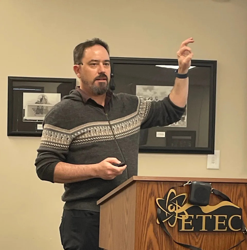
Stephen Jesse speaks for Friends of ORNL about efforts using advanced microscopes to make quantum materials.
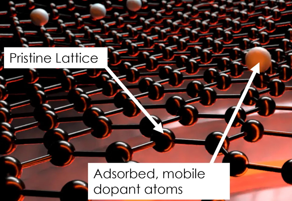
Dopant atoms of tin “planted” by the ORNL synthescope in graphene, a single layer of carbon atoms arranged in a hexagonal lattice like chicken wire.
This article originally appeared on Oakridger: ORNL scientist talks on atomic building blocks for quantum computers