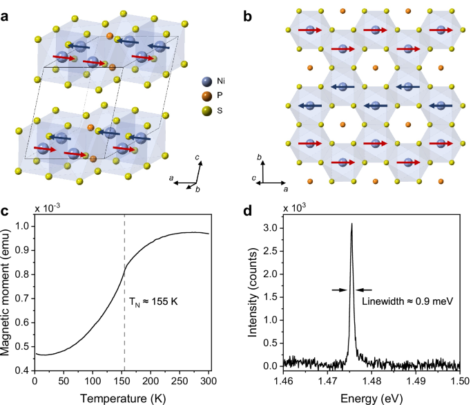
NiPS3 has a monoclinic structure, where Ni ions are octahedrally coordinated by six S ligands, and the resulting structure consists of NiPS3 layers that are held together by weak vdW forces (Fig. 1)22. This layered structure is amenable to cleaving into few-layer flakes using micromechanical exfoliation (Supplementary Fig. S1). Below the TN of 155 K, NiPS3 adopts a colinear zig-zag AFM structure, with spins pointing primarily along the a-axis, with a small out-of-plane component23. Magnetic susceptibility measurements of bulk NiPS3 crystals exhibit a clear paramagnetic to AFM phase transition at 155 K (Fig. 1c).
Fig. 1: Crystal structure and characterization of NiPS3.
a Side and b top views of the crystal structure with the arrows indicating the antiferromagnetic order of NiPS3. c Magnetic susceptibility versus temperature showing the transition from the paramagnetic to the antiferromagnetic state at 155 K (measured with an in-plane field of 104 Oe). d Photoluminescence spectrum of NiPS3 at 4 K, showing the exciton peak at 1.476 eV with a linewidth of 0.9 meV.
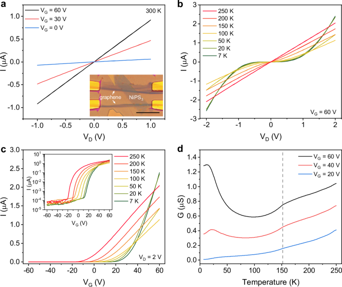
In order to achieve electrical transport below the Néel temperature, we fabricate all vdW NiPS3 FETs with hBN as the gate dielectric and few-layer graphene (FLG) as the source and drain contacts using all-dry flake pick-up and transfer methods (see Methods). The resulting pristine interfaces between the NiPS3 channel and the FLG contacts and hBN dielectric result in ohmic transport down to 100 K (Fig. 2). Recent studies show that FLG is among the best contact materials to 2D magnetic semiconductors (e.g., CrI3, NiI2, VI3, CrPS4), likely due to the alignment of the FLG work function relative to the conduction band of these materials16,24,25,26,27. Moreover, in our NiPS3 FETs the current modulation remains high (ION/IOFF ≈ 105) from room temperature down to 2 K with µFE in the range of 1.3-4.5 cm2 V−1 s−1 over the entire temperature range (Fig. 2c and Supplementary Fig. S2). Plotting conductance as a function of temperature results in a kink at 155 K, which corresponds to the paramagnetic to AFM phase transition (Fig. 2d), as has been also observed in other 2D AFM semiconductors such as NiI225, CrSBr28,29, and CrPS427. At high gate bias (VG), the conductance of the NiPS3 devices increases with decreasing temperature below ≈100 K. The increasing conductance can likely be attributed to the suppression of spin-fluctuations and scattering events due to the emerging long-range AFM order below TN25,27,28.
Fig. 2: Variable-temperature charge transport in NiPS3.
a Output curves for a NiPS3 field-effect transistor at 300 K at different gate voltages demonstrating an Ohmic response. The inset shows a picture of the device with a scale bar of 10 μm. b Variable-temperature output curves for the same device at VG = 60 V. c Transfer characteristics for the NiPS3 field-effect transistor at various temperatures with VD = 2 V. The inset shows the results on a log scale. d Conductance versus temperature at three gate voltages (VG = 20, 40, 60 V) showing a kink at TN of 155 K (vertical dashed line).
To further demonstrate the utility of our functional FET devices at cryogenic temperatures, we performed photocurrent measurements of NiPS3. A direct observation of photocurrent generation from magnetic excitons, which is the reverse process compared to electroluminescence, highlights the high quality of our NiPS3 FETs. In particular, we measured spectrally resolved photocurrent at 7 K and observed two lines at 1.476 eV and 1.504 eV (Supplementary Fig. S2c), which we assign to the magnetic exciton and its two-magnon sideband, respectively. The linewidth of these features is broader compared to PL measurements (Fig. 1d), but in the case of photocurrent measurements, the linewidth is limited by the resolution of the monochromator, rather than the intrinsic properties of NiPS3.
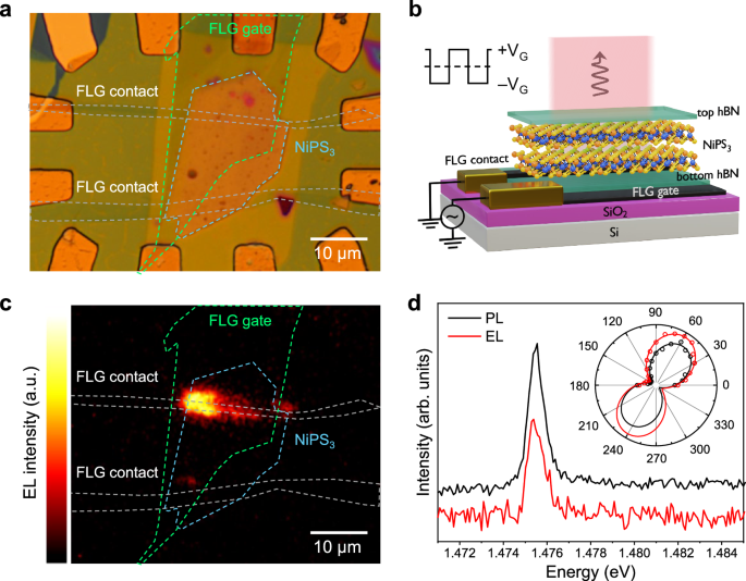
In order to drive EL at low applied gate voltage, we fabricated NiPS3 FETs such that all device components, including electrodes and dielectric layers, are formed by thin vdW materials. Specifically, we used local gating from FLG that is capacitively coupled to NiPS3 through an hBN dielectric (Fig. 3a, b). Compared to FETs with global Si gate through 300 nm SiO2 (shown in Fig. 2), the local-gate design allows decreased gate voltage, but otherwise the charge transport characteristics of NiPS3 remain unchanged (Supplementary Figs. S3 and S4). Lower gate voltages enable EL to be driven via application of a square wave voltage profile to the gate electrode that is capacitively coupled to the FET channel by grounding both the source and drain electrodes. Switching of the gate voltage polarity modulates the quasi-Fermi level in the NiPS3 channel, resulting in rapid band bending. When this process is driven at MHz frequencies, a fraction of the induced free carriers remains in the channel, where they subsequently recombine with the oppositely charged carriers injected from the grounded electrodes30,31,32,33,34. This electron-hole recombination results in EL within a short time interval (determined by the lifetime of the carriers) from the sharp edges of the gate voltage square wave. The efficiency of the process is determined by intrinsic doping, trap density, carrier mobility in the semiconductor, and contact metal work function. The latter partially determines the contact resistance, which we have not estimated in the present study, as it requires multi-terminal NiPS3 – FLG devices that are not necessary for EL measurements.
Fig. 3: Electroluminescence of NiPS3.
a NiPS3 field-effect transistor device with a local few-layer graphene gate. b Schematic of the device and biasing scheme. c Electroluminescence image, demonstrating emission near the few-layer graphene contacts (T = 2 K) d Comparison of the photoluminescence and electroluminescence spectra of NiPS3. The inset shows the polarization dependence, highlighting a high degree of linear polarization for both PL and EL. The EL spectra were recorded using a square wave voltage signal with an amplitude of 6.5 V and a frequency of 14 MHz.
We further studied the evolution of the EL intensity as a function of temperature and observed that, similar to PL35, the EL intensity drops at higher temperature and the EL is suppressed above 90 K (Supplementary Fig. S5). Comparing the temperature evolution of EL and PL intensities shows slightly faster decrease for EL, which is likely a result of Joule heating associated with the electrical excitation (we estimate the corresponding temperature rise to be less than ~10 K). Next, we studied the dependence of the EL on the parameters of the applied square wave, such as amplitude and frequency. We find that the intensity of emission first increases linearly for smaller excitation amplitudes (Supplementary Fig. S6), then saturates, and finally declines with further increase in the amplitude. Although saturation is often associated with defect emission, our observed saturation of NiPS3 EL intensity with voltage amplitude can be attributed to saturation of the density of trapped carriers during the half cycle of the opposite polarity voltage, as has been reported in previous work on AC-driven EL emitters30. The decline in EL intensity at the highest voltage amplitudes coincides with a sharp increase in the linewidth, which we interpret as Joule heating. We also observed negligible changes in the energy of the magnetic exciton and an increase in the linewidth at high excitation amplitudes and frequencies, which is also likely attributable to Joule heating of the sample (Supplementary Figs. S6 and S7).
In order to spatially resolve the electroluminescence, we imaged the NiPS3 device using a high-sensitivity camera. We observe that the EL is located near the graphene contacts and spectrally matches the ultranarrow magnetic excitonic peak for antiferromagnetically ordered NiPS3 (Fig. 3c, d). When both FLG contacts are grounded, we observe emission near each contact; however, the distribution of its intensity is inhomogeneous. The observed inhomogeneities could arise from slight variations in thickness of the flakes, particularly NiPS3 and the bottom hBN dielectric, as well as from lateral voltage drops across the bottom graphene flake used as a local gate. Homogeneous and larger area EL can be achieved by using high-density interdigitated contacts, as has been shown previously for transition metal dichalcogenides30.
In PL measurements, we found that the linear polarization of the magnetic exciton emission (at T = 2 K) shows strong two-fold anisotropy with a high degree of linear polarization (ρ = 0.84), which is calculated as ρ = (Ia – Ib)/(Ia + Ib), where Ia (Ib) is the intensity parallel to the a-axis (b-axis) (Fig. 3d inset). This observation is in line with previous PL studies of NiPS3, which revealed coupling of the polarization of magnetic excitons with the induced electrical polarization and Néel vector of the AFM order13,15. Similar to PL, we find that NiPS3 EL also has a strong degree of linear polarization (ρ = 0.78) that is aligned along the same polarization direction as the PL measurements (Fig. 3d). The slightly lower degree of polarization as well as the ~3.9° rotation of the polarization direction of the EL compared to PL can be attributed to minor variations of the Néel vector direction within the NiPS3 flake.
The antiferromagnetic semiconducting properties of NiPS3 result in coherent excitons that are entangled with the underlying AFM order. By maintaining measurable charge transport in NiPS3 FETs below TN, we can exploit the ultranarrow linewidths of these magnetic excitons to achieve EL with performance superior to traditional nonmagnetic 2D semiconductors such as transition metal chalcogenides. In particular, the EL linewidth of NiPS3 (0.9 meV) is lower than the homogeneous broadening of excitons in MoS2 and WSe2, which is determined by exciton-phonon interactions (1–5 meV)19,20,21. In addition, the EL of NiPS3 is highly linearly polarized, where the polarization angle can be controlled by the in-plane magnetic field15. The processing methods introduced here can also be applied to alternative electronic device geometries, such as vertical heterostructures36,37 to further exploit the opto-spintronic properties of 2D NiPS3.
In summary, we have utilized all-dry fabrication methods to achieve semiconducting charge transport in NiPS3 at cryogenic temperatures down to 2 K, which enables electrical detection of the AFM transition at 155 K. The local-gate FET geometry further facilitates capacitively coupled EL from the quantum-entangled magnetic excitons of NiPS3 with an ultranarrow linewidth of less than 1 meV and a high degree of linear polarization (ρ = 0.78), providing distinct advantages compared to EL from traditional nonmagnetic transition metal dichalcogenide semiconductors. Unlike optical pumping, electrical pumping can serve as the basis of other device concepts, including the use of ferromagnetic contacts (e.g., Fe3GeTe2) for the injection of spin-polarized currents38. In this manner, this work establishes a 2D platform for fundamental studies of the interactions among light, charge, and spin in addition to vdW opto-spintronic applications.