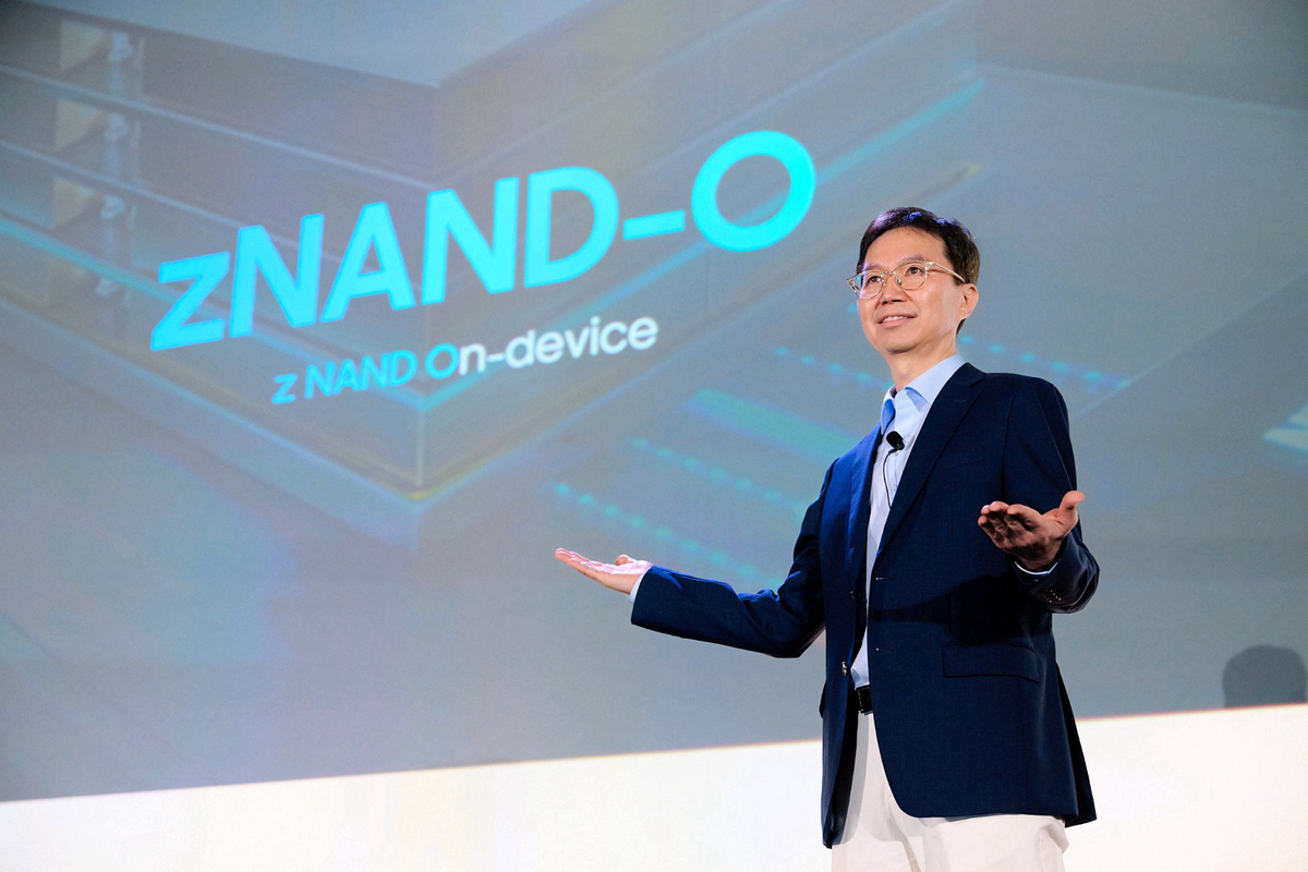
 Lee Jin-yeop, Vice President of Samsung Electronics’ Flash Development Division, gives a presentation at “FMS 2026” held in Silicon Valley, U.S., on the 4th (local time). Samsung Electronics
“Samsung is back.”
Kim Kyung-ryun, vice president of Samsung Electronics’ (005930.KS) DRAM development division, expressed confidence in the company’s “technology gap superiority” as he introduced “z High Bandwidth Memory (zHBM)” at FMS 2026, held in the United States on the 4th.
zHBM, Samsung Electronics’ new memory architecture, is a core technology aimed at the artificial intelligence (AI) accelerator market, which is rapidly reorganizing toward application-specific integrated circuits (ASIC).
Recent AI models are rapidly evolving beyond generative AI that answers questions toward “agentic AI” that plans, reasons and acts on its own. As AI models become more advanced, the volume of data they must process is also surging. In particular, the burden on memory chips is growing as not only data generated during long conversations and complex reasoning processes but also the “KV cache,” which stores and utilizes previous information, expands in size.

For this reason, AI’s competitiveness is shifting beyond computing performance to how efficiently vast amounts of data can be stored and how quickly they can be delivered to AI accelerators. No matter how high the performance of xPUs such as graphics processing units (GPU) and tensor processing units (TPU), which handle the core computations of AI accelerators, the overall quality of AI services is limited if data is not supplied in time.
Samsung Electronics’ strategy is to firmly grasp the leadership of the AI memory market by solving this data bottleneck problem through chips that apply cutting-edge new technologies such as zHBM, z NAND-O and V10 BV-NAND.
zHBM applies an innovative structure that shortens the distance between the AI accelerator and memory. While conventional HBM places memory beside the GPU, zHBM minimizes the data travel distance through a structure that stacks memory directly on top of the GPU. It also strengthens inter-chip connection efficiency and thermal management performance by utilizing hybrid copper bonding (HCB). When zHBM is applied, performance improves up to eight times and power efficiency up to three times compared with HBM5 (the eighth generation), which will not be released until next year.
“With the existing packaging structure, there are limits to narrowing the physical distance between the accelerator chip and memory,” Kim said. “We will overcome this barrier by implementing gate-all-around (GAA) transistors for the first time in HBM and introducing the foundry 2-nanometer (nm, one billionth of a meter) ultra-fine process.”
z NAND-O, aimed at the on-device AI era, is also a technology that will greatly boost the performance of storage devices. Running AI directly on devices such as smartphones requires large storage capacity and fast data processing capability even in small spaces. z NAND-O applies 3D packaging technology that vertically stacks V-NAND chips using the through-silicon via (TSV) method, achieving high storage density and data processing speed. It supports the execution of AI functions inside the device without a cloud connection, offering significant advantages in terms of personal information protection.
Samsung also presented a solution for the era of exploding data through V10 BV-NAND. This technology implements a stacking structure of more than 400 layers, enabling more data to be stored in the same area. Through this, it achieved about 58% higher integration density than previous-generation chips. In data centers, it can improve space and power efficiency while storing more information, while in mobile devices it enables the implementation of thinner and lighter high-capacity storage solutions.
With its three-dimensional memory architecture at the forefront, Samsung Electronics is expected to seize leadership in the coming ASIC era and solidify its status as Big Tech’s top partner. Recently, Google, Amazon, Microsoft and Meta have been moving away from Nvidia’s GPU-centered AI accelerators and expanding the adoption of ASICs optimized for their own AI models. Google is utilizing TPUs optimized for search, cloud and generative AI services, while Amazon is expanding its own AI chips Trainium and Inferentia. Meta is also enhancing data center operating efficiency by introducing the Meta Training and Inference Accelerator (MTIA).
Samsung Electronics is the world’s only integrated device manufacturer (IDM) capable of providing a “one-stop solution” spanning memory, logic (semiconductor design), foundry (contract chip manufacturing) and packaging (back-end processing), and it plans to preempt not only the next-generation AI accelerator market but also the high-performance computing (HPC) market. “We will provide integrated services from product design to mass production, supporting the implementation of customized AI semiconductors so that customers can shorten development periods and optimize performance and power efficiency,” a key Samsung official said.
 A view of Samsung Electronics’ booth at “FMS 2026” held in Silicon Valley, U.S., on the 4th (local time). Samsung Electronics