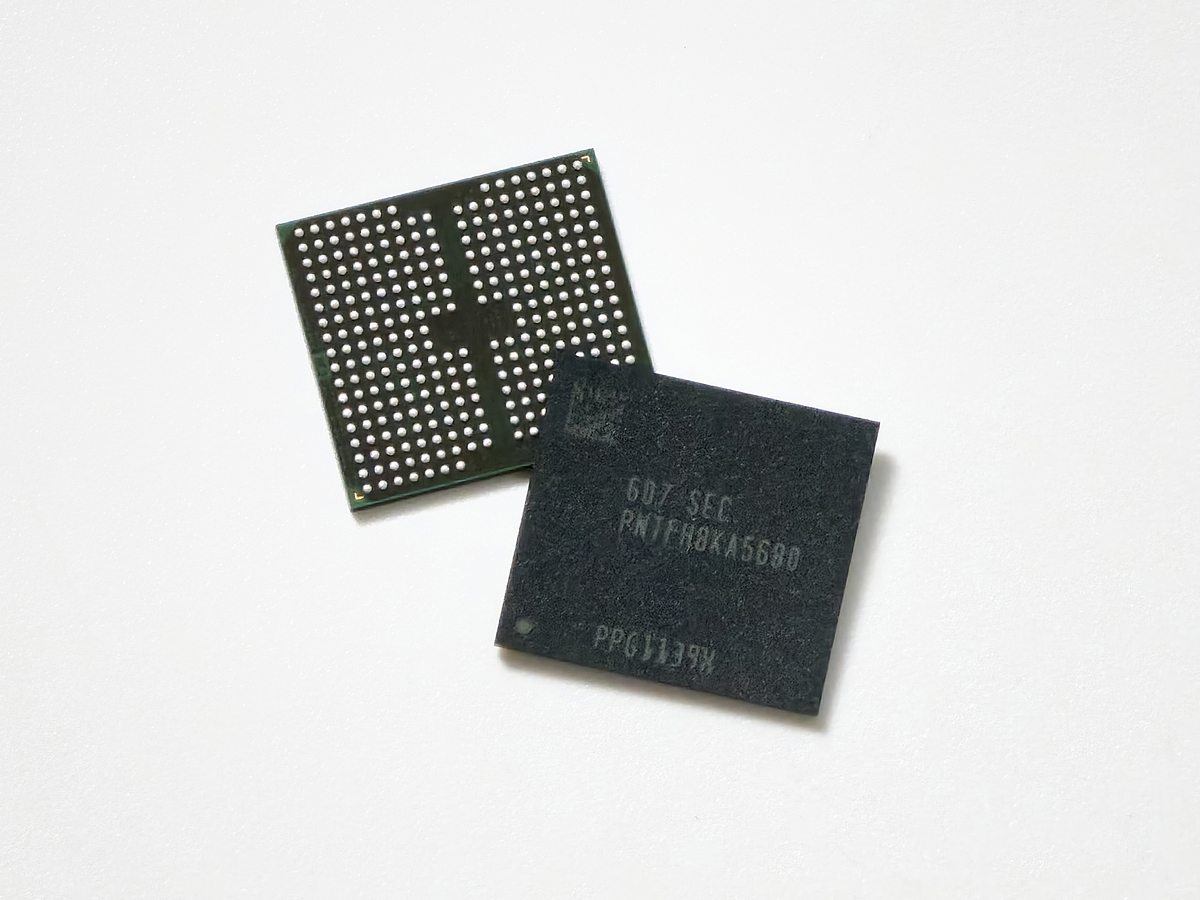
 V10 BV-NAND. Samsung Electronics
Samsung Electronics (005930.KS) is aiming to lead the DRAM and NAND flash markets with next-generation three-dimensional (3D) technology. Its strategy is to resolve memory bottlenecks by stacking multiple layers of high-bandwidth memory (HBM) and NAND flash, positioning the company to lead the agentic AI era.
At FMS 2026, which opened on the 4th at the Santa Clara Convention Center in California, Samsung Electronics unveiled for the first time its 3D memory architectures—the design structure that determines how a chip operates—’zHBM’ and ‘z-NAND-O.’ These are next-generation memory technologies designed to respond to growing demand for high-performance computing (HPC) and AI infrastructure, and to maximize the performance and power efficiency of AI systems.
HBM is a memory chip made by stacking multiple layers of DRAM and is regarded as the most important chip in the era of artificial intelligence (AI) development. zHBM, which follows the eighth-generation HBM (HBM5) currently under development, is a next-generation 3D architecture that vertically stacks HBM atop AI accelerators such as graphics processing units (GPUs) and application-specific integrated circuits (ASICs).
 Kim Kyung-ryun, executive vice president of Samsung Electronics’ DRAM Design Team, introduces next-generation technology at FMS 2026 on Feb. 4 local time. Correspondent Kim Chang-young
As the focus of AI shifts from training to inference, data throughput has surged, driving the continued evolution of HBM technology to minimize AI bottlenecks. Until now, bottlenecks have been reduced by attaching multiple HBM units to AI chips, but this approach has hit limits in stacking technology and bandwidth (the amount of data transmitted per second) expansion. To overcome this, Samsung Electronics devised a method of stacking the HBM itself up to four layers high.
Samsung Electronics viewed 3D as the only way to resolve HBM bottlenecks in a situation where TSV (Through Silicon Via) technology is already being used. TSV is a packaging technology that shaves DRAM chips to less than half the thickness of ordinary paper and then connects the top and bottom of the chips with electrodes by drilling fine holes, rather than connecting the chips with wires. It achieves high capacity by stacking memory chips.
Samsung Electronics said that zHBM can deliver up to eight times higher performance than HBM5 by minimizing data travel distance to maximize bandwidth and power efficiency. It can improve power efficiency by up to three times compared with the previous generation and reduce thermal resistance by more than half. Another characteristic is that customized designs are possible according to features required by customers, such as capacity expansion and accelerator performance enhancement, in the interlayer located between the memory and the AI accelerator.
On the same day, Samsung Electronics also presented ‘z-NAND-O,’ a next-generation memory technology that implements 3D technology in NAND flash, just as zHBM does. By applying 3D packaging technology that vertically stacks multiple V-NAND chips using TSV, it achieves space efficiency, high performance, and low power consumption, while also providing high bandwidth and response speed. As a technology that can simultaneously resolve DRAM’s capacity shortage and NAND flash’s low bandwidth, it can deliver high capacity, high bandwidth, and fast response speed at the same time.
With the arrival of the agentic AI era, in which AI reasons on its own, the throughput and speed of processing inference data have become important, and the role of NAND flash in AI infrastructure has grown. Samsung Electronics explained that z-NAND-O is optimized for on-device AI, which runs AI on personal devices, and can deliver high performance in real-time data processing.
Samsung Electronics also unveiled ‘V10 BV-NAND,’ its 10th-generation V-NAND with more than 400 vertically stacked layers, the first in the industry. Through wafer bonding technology and three-tier stack technology, it achieves ultra-high stacking and improves memory density by about 58% compared with the previous generation, allowing more data to be stored in the same area.